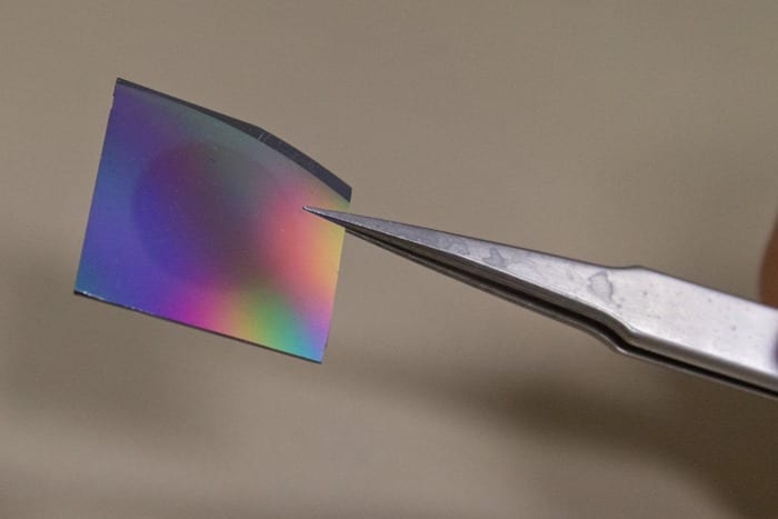
A silicon sample after being removed from the cylinder.
Reduced costs for industry
A team of researchers from the Nanoengineering Research Centre (CRNE) and the Department of Electronic Engineering at the Universitat Politècnica de Catalunya · Barcelona Tech (UPCn has found a way to make the manufacture of crystalline silicon materials faster and more affordable. The results of their research have recently been published in the online version of the landmark journal Applied Physics Letters.
Thin crystalline silicon wafers measuring around 10 µm (micres) are costly but also very sought after in the field of microelectronics, especially in view of the growing demand for 3D circuit integration with microchips. Silicon wafers also have potential photovoltaic applications in the medium term in the conversion of sunlight to electricity and the production of more affordable, more flexible and lighter solar cells.
In recent years, techniques have been developed to obtain increasingly thinner crystalline silicon wafers from monocrystalline cylindrical ingots. Layers cut from the ingots using a multithreaded saw impregnated with abrasive material have a minimum thickness of around 150 µm. Obtaining wafers that are any thinner is more complicated, as existing methods only allow such wafers to be obtained one at a time. Furthermore, 50% of the silicon is lost in the process.
The technology developed by the research team – David Hernández, Trifon Trifonov and Moisés Garín, led by Professor Ramon Alcubilla – enables a large number of crystalline layers, controlled for thickness, to be produced from a single crystalline silicon wafer in just a single step. The outcome is a kind of crystalline silicon “millefeuille” produced more efficiently, more rapidly and more affordably than by existing methods.
The Latest Bing News on:
Thin crystalline silicon wafers
- New research demonstrates potential of thin-film electronics for flexible chip designon April 24, 2024 at 8:00 am
The mass production of conventional silicon chips relies on a successful business model with large "semiconductor fabrication plants" or "foundries." New research by KU Leuven and imec shows that this ...
- Indian imports of monocrystalline silicon wafers from China have surged, why?on April 16, 2024 at 7:42 pm
India almost doubled its imports of silicon wafers from China in 2023, highlighting India's expansion in solar cells and modules amid rising dependence on China's materials.
- How Much Do Solar Panels Cost In 2024?on April 15, 2024 at 11:19 pm
Unlike monocrystalline cells, however, the polycrystalline variety is comprised of fragmented silicon crystals cut into wafer ... thin-film cells use amorphous silicon, which isn’t crystalline.
- Switching to solar? We explain three main types of solar panelson April 13, 2024 at 1:31 pm
The silicon ingot is then sliced into thin wafers to make solar cells ... Generally less efficient than crystalline silicon panels Degradation is around 200% of what you’d get from other ...
- Different Types Of Consumer Solar Panels (And Which Is Right For You)on March 27, 2024 at 10:34 am
According to estimates by the U.S. Department of Energy, CdTe (cadmium telluride) thin-film solar ... up of multiple silicon crystals which are melted together, creating wafers that result in ...
- Interference-based detection of nucleic acid targets on optically coated siliconon February 5, 2024 at 10:57 pm
Figure 1: Schematic representation of the coated-silicon hybridization-based biosensor. The base substrate of the chip is crystalline silicon ... as a function of thin-film formation.
- Mining And Refining: Quartz, Both Natural And Syntheticon September 6, 2023 at 12:54 am
Once its unusual electrical properties were understood, crystalline quartz ... Its abundance of silicon makes it the perfect feedstock for silicon wafer production, and fused quartz glass of ...
- Photovoltaic Device Teamon August 17, 2020 at 1:38 am
The use of thin crystalline silicon as a bottom cell provides high efficiency and ... 5】GaAs/Si-based three-junction smart stack cell Apparatus that etches a single side of the wafer by spin rotation.
- Wafer and Thin Film Instrumentation Informationon August 14, 2020 at 4:51 am
Wafer and thin film instrumentation consists of devices such as critical ... works on a similar principal to the SEM. They study surfaces of crystalline materials and gather data solely from a ...
- From Sand To Waferson April 17, 2019 at 5:00 pm
Silicon wafers are fundamental in manufacturing the ... in polycrystalline (“poly”) and amorphous (glass-like non-crystalline) forms is used in photovoltaic (solar) cells and thin film transistors.
The Latest Google Headlines on:
Thin crystalline silicon wafers
[google_news title=”” keyword=”thin crystalline silicon wafers” num_posts=”10″ blurb_length=”0″ show_thumb=”left”]
The Latest Bing News on:
Crystalline silicon materials
- Imperial Academic Secures €2.4m European Funding to Enhance Solar Harvesting Technologyon April 26, 2024 at 4:40 pm
Professor Jenny Nelson has won a prestigious European Research Council grant to learn lessons from plants and apply them to solar technologies.She will use the grant to unpick how plants convert ...
- Photovoltaic Research Challenges: Overcoming Hurdles in Solar Technologyon April 24, 2024 at 7:44 am
Solar photovoltaic (PV) technology has evolved in the past few years, particularly in solar panels and systems. However, researchers and institutions are actively working to overcome limitations to ...
- Quartz, cobalt, and the waste we leave behindon April 24, 2024 at 1:59 am
Some time before the first dinosaurs, two supercontinents, Laurasia and Gondwana, collided, forcing molten rock out from the depths of the Earth. As eons passed, the liquid rock cooled and geological ...
- Fantastic plasticon April 20, 2024 at 2:33 am
Much of the early work on photoactive materials for photovoltaics focused on crystalline silicon, which dominates the commercial solar-energy field today. Several other materials, such as ...
- RNWEF REC Silicon ASAon April 19, 2024 at 4:04 am
REC Silicon ASA, together with its subsidiaries, produces and sells silicon materials for the solar ... including NextSi used for multi crystalline and monocrystalline solar ingot and wafer ...
- Solar Laser Drilling Market to Reach $6,659.2 Million Globally by 2032 at 9.1% CAGR: Allied Market Researchon April 17, 2024 at 7:30 am
The growing adoption of renewable energy, rising demand for sustainable manufacturing, and the advancements in laser technology are anticipated to drive the growth of the global solar laser drilling ...
- Novel Quantum Effect Observed in a Crystalline Materialon April 10, 2024 at 5:00 pm
Physicists have observed a novel quantum effect termed “hybrid topology” in a crystalline material ... Second, simple and elemental material systems (like silicon for conventional electronics) that ...
- Thermally engineering templates for highly ordered self-assembled materialson February 14, 2024 at 12:43 pm
that is at least 100 times less thermally conductive than crystalline silicon. The template material's low thermal conductivity minimizes the flow of heat in the "wrong" direction. "The thermal ...
- Solar panel world record smashed with ‘miracle material’on November 8, 2023 at 3:25 am
“The emergence of crystalline silicon-perovskite tandem technology ... Perovskite has been hailed as a “miracle material” for its potential to revolutionise everything from high-speed ...
- From smart contact lenses to supercooled siliconon March 19, 2019 at 3:03 am
But because of silicon's high melting point (1,414 ... building block for preparing highly ordered discotic liquid-crystalline materials that can be subsequently functionalized by standard ...
The Latest Google Headlines on:
Crystalline silicon materials
[google_news title=”” keyword=”crystalline silicon materials” num_posts=”10″ blurb_length=”0″ show_thumb=”left”]


