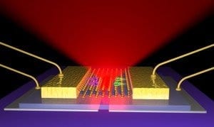
The LED is based off of two-dimensional, flexible semiconductors, making it possible to stack or use in much smaller and more diverse applications than current technology allows.
Most modern electronics, from flat-screen TVs and smartphones to wearable technologies and computer monitors, use tiny light-emitting diodes, or LEDs. These LEDs are based off of semiconductors that emit light with the movement of electrons. As devices get smaller and faster, there is more demand for such semiconductors that are tinier, stronger and more energy efficient.
University of Washington scientists have built the thinnest-known LED that can be used as a source of light energy in electronics. The LED is based off of two-dimensional, flexible semiconductors, making it possible to stack or use in much smaller and more diverse applications than current technology allows.
“We are able to make the thinnest-possible LEDs, only three atoms thick yet mechanically strong. Such thin and foldable LEDs are critical for future portable and integrated electronic devices,” said Xiaodong Xu, a UW assistant professor in materials science and engineering and in physics.
Xu along with Jason Ross, a UW materials science and engineering graduate student, co-authored a paper about this technology that appeared online March 9 in Nature Nanotechnology.
Most consumer electronics use three-dimensional LEDs, but these are 10 to 20 times thicker than the LEDs being developed by the UW.
“These are 10,000 times smaller than the thickness of a human hair, yet the light they emit can be seen by standard measurement equipment,” Ross said. “This is a huge leap of miniaturization of technology, and because it’s a semiconductor, you can do almost everything with it that is possible with existing, three-dimensional silicon technologies,” Ross said.
The UW’s LED is made from flat sheets of the molecular semiconductor known as tungsten diselenide, a member of a group of two-dimensional materials that have been recently identified as the thinnest-known semiconductors. Researchers use regular adhesive tape to extract a single sheet of this material from thick, layered pieces in a method inspired by the 2010 Nobel Prize in Physics awarded to the University of Manchester for isolating one-atom-thick flakes of carbon, called graphene, from a piece of graphite.
In addition to light-emitting applications, this technology could open doors for using light as interconnects to run nano-scale computer chips instead of standard devices that operate off the movement of electrons, or electricity. The latter process creates a lot of heat and wastes power, whereas sending light through a chip to achieve the same purpose would be highly efficient.
“A promising solution is to replace the electrical interconnect with optical ones, which will maintain the high bandwidth but consume less energy,” Xu said. “Our work makes it possible to make highly integrated and energy-efficient devices in areas such as lighting, optical communication and nano lasers.”
The research team is working on more efficient ways to create these thin LEDs and looking at what happens when two-dimensional materials are stacked in different ways. Additionally, these materials have been shown to react with polarized light in new ways that no other materials can, and researchers also will continue to pursue those applications.
The Latest on: LEDs
[google_news title=”” keyword=”LEDs” num_posts=”10″ blurb_length=”0″ show_thumb=”left”]
via Google News
The Latest on: LEDs
- Microdisplay can monitor brain activity in real-timeon May 1, 2024 at 4:11 am
Engineers and physicians from University of California San Diego and Massachusetts General Hospital (MGH) have developed a thin film display device that combines an electrode grid and special GaN LEDs ...
- Mother sea turtles arrive at Fort Myers Beachon April 30, 2024 at 10:34 am
The mama sea turtles officially arrived at Fort Myers Beach on Tuesday. Officials are reminding you to please update your exterior lighting to amber and red LEDs in a downward direction, shielding the ...
- Infinix GT 20 Pro gaming phone debuts with a better display and a new set of LEDson April 29, 2024 at 8:21 pm
Infinix debuted its first gaming phone last year, which was also on a budget, and its successor just went official.
- The horticultural lighting revival gains groundon April 29, 2024 at 2:05 pm
Both Signify and ams Osram reported ongoing growth in their quarterly calls last week. But will electricity prices continue to decline in their favor?
- illumiPure Inc. Achieves IEC 62471 Exempt Certification, Setting New Standard in Lighting Technologyon April 29, 2024 at 11:01 am
HOUSTON, TX / ACCESSWIRE / April 29, 2024 / illumiPure, Inc., a leader in innovative LED solutions, is proud to announce that its patented CleanWhite® 405 nm and 405/470 nm ...
- Infinix GT 20 Pro 5G launched with MediaTek Dimensity 8200 SoC, customisable LEDs: price, specificationson April 28, 2024 at 1:32 pm
Infinix GT 20 Pro 5G price has been revealed officially in Saudi Arabia. Check out to know about the Infinix GT 20 Pro specifications.
- Infinix GT 20 Pro arrives with Dimensity 8200 Ultimate, 144Hz screen, and customizable LEDson April 27, 2024 at 5:00 pm
It also features a Mecha Loop LED interface, meaning the phone's rear panel sports customizable RGB LEDs supporting eight color combos and four lighting effects. The game lighting effects support ...
- Update your lighting system with LEDson April 25, 2024 at 7:56 am
As more light bulbs are being removed from the market, what are the best options for keeping your lighting system up to date?
- SemiLEDs Corp LEDSon April 24, 2024 at 12:39 pm
Morningstar Quantitative Ratings for Stocks are generated using an algorithm that compares companies that are not under analyst coverage to peer companies that do receive analyst-driven ratings ...
- Banned in the U.S: Healthy Light Bulbson April 24, 2024 at 12:00 pm
In a retrograde move, the U.S. Department of Energy (DOE) has just issued a final rule that, effective June 25 2028, will firmly cement the dominance of unhealthy blue-pump LED light bulbs. It is ...
via Bing News


