


Engineers build cutting-edge photonic devices using standard chip-making process
The future of computing may lie not in electrons, but in photons – that is, in microprocessors that use light instead of electrical signals. But these so-called photonic devices are typically built using customized methods that make them difficult and expensive to manufacture.
Now, engineers have demonstrated that low power photonic devices can be fabricated using standard chip-making processes. They have achieved what the researchers dub a major milestone in photonic technology. The work will be presented at this year’s Optical Fiber Communication (OFC) Conference and Exposition, being held March 9-13 in San Francisco.
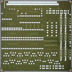
The two new devices – a modulator and a tunable filter – are as energy-efficient as some of the best devices around, the researchers say, and were built using a standard IBM advanced Complementary Metal-Oxide Semiconductor (CMOS) process – the same chip-making process used to build many commercially available chips, some of which are found in Sony’s Playstation 3 and also in Watson, the supercomputer that won Jeopardy! in 2011.
“As far as we know, we’re the first ones to get silicon photonics natively integrated into an advanced CMOS process and to achieve energy efficiencies that are very competitive with electronics,” said Mark Wade of the University of Colorado, Boulder, who will present his team’s work at OFC. Wade’s co-authors include researchers from the Massachusetts Institute of Technology and the University of California, Berkeley.
Quenching a Thirst for Power
Moore’s Law says that the number of transistors that can fit on a chip doubles every two years, resulting in the exponential rise in computing power we have seen over the last few decades. But even as transistors continue to shrink, Moore’s Law may be reaching its limits, due to the fact that the devices are requiring more power to run, which leads to overheating.
Such thirst for power is especially problematic for the communication link between a computer’s central processing unit and its memory.
“It’s gotten to the point where it takes too much energy and that limits your computational power,” Wade said.
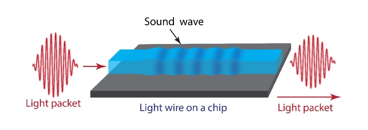
A solution to this problem may lie in photonics, which researchers anticipate will be at least 10 times more energy efficient than electronics. Chip-to-chip communication links using these photonic devices could have at least 10 times higher bandwidth density, meaning they can transmit much more information using a smaller amount of space. That’s because different optical signals can share the same optical wire, whereas sending multiple electrical signals either requires multiple electronic wires or schemes that require more chip space and energy.
But so far, Wade explains, photonic devices used in chip-to-chip communication have been primarily custom-built using specialized methods, limiting their commercial applicability. And devices that have been created with more standardized techniques rely on older technology, which limits their ability to compete with cutting-edge electronics.
On the Road to Commercialization
The ability to produce high-performing photonic devices using the CMOS process means chip designers will not have to be specialists to design photonic devices, Wade explained, which will hopefully accelerate the commercialization of photonic technology.
The Latest on: Photonics
[google_news title=”” keyword=”Photonics” num_posts=”10″ blurb_length=”0″ show_thumb=”left”]
via Google News
The Latest on: Photonics
- ECTC 2024 to highlight emerging technologies enabling heterogeneous integration and photonicson April 30, 2024 at 10:55 am
The IEEE Electronic Components and Technology Conference (ECTC) is the world’s leading forum for unveiling, discussing, and exhibiting the latest advancements in microelectronics packaging and ...
- IPGP Stock Earnings: IPG Photonics Beats EPS, Misses Revenue for Q1 2024on April 30, 2024 at 10:05 am
IPGP stock results show that IPG Photonics beat analyst estimates for earnings per share but missed on revenue for the first quarter of 2024.More From InvestorPlace The #1 AI Investment Might Be This ...
- IPG Photonics' (IPGP) Q1 Earnings Beat, Revenues Decrease Y/Yon April 30, 2024 at 8:50 am
Sales decreased 16% in North America, 38% in China and 23% in Japan on a year-over-year basis. Moreover, sales decreased 21% year over year in Europe. IPG Photonics reported a gross margin of 38.7%, ...
- IPG Photonics (NASDAQ:IPGP) Misses Q1 Sales Targetson April 30, 2024 at 7:40 am
Fiber laser manufacturer IPG Photonics (NASDAQ:IPGP) missed analysts' expectations in Q1 CY2024, with revenue down 27.4% year on year to $252 million. Next quarter's revenue guidance of $255 million ...
- Lasers, Lenses & Light: A Showcase of Fitzpatrick Institute Photonics Research for the Communityon April 30, 2024 at 7:26 am
Duke has a long tradition as a leader in research on light. One Duke alumnus, Charles Townes, went on to win the Nobel Prize for Physics for his discovery involving lasers. Over the past two decades, ...
- IPG Photonics Appoints Gitin As CEOon April 30, 2024 at 7:19 am
IPG Photonics Corp. (IPGP) announced the appointment of Mark Gitin, as the Chief Executive Officer and a member of the ...
- IPG Photonics Shares Edge Down 5.1% on 1Q Results, 2Q Guidanceon April 30, 2024 at 6:23 am
By Denny Jacob IPG Photonics shares edged down 5.1% in premarket trading on first-quarter results that came in sharply lower from a year earlier ...
- IPG Photonics Announces First Quarter 2024 Financial Resultson April 30, 2024 at 6:05 am
Delayed E-mobility Investments and Soft Industrial Demand Negatively Impacted ResultsStrong Operating Cash Flow Benefited from Working Capital ...
- IPG Photonics Taps Gitin to Succeed Scherbakov as CEOon April 30, 2024 at 5:26 am
By Colin Kellaher IPG Photonics has hired Mark Gitin to succeed co-founder Eugene Scherbakov as chief executive of the maker of high-power fiber lasers ...
- IPG Photonics reports mixed Q1 results; initiates Q2 outlookon April 30, 2024 at 5:06 am
Q1 GAAP EPS of $0.52 beats by $0.04. Revenue of $252M (-27.4% Y/Y) misses by $1.71M. Business Outlook and Financial Guidance "Despite a challenging first quarter, our book-to-bill was slightly above ...
via Bing News
