


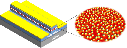
Researchers from the University of California, Santa Barbara have reported a breakthrough in chip design that integrates electronic and photonic components and could lead to smaller, lighter, more power-efficient and less expensive microsystems of the kind used in radar, communications, imaging and sensing devices.
In work funded by the Defense Advanced Research Projects Agency, the researchers have managed to place billions of light-emitting dots, or “quantum dots,” directly onto silicon, a process that avoids more involved and expensive procedures, DARPA said in a release. The research was done as part of DARPA’s Electronic-Photonic Heterogeneous Integration (E-PHI) program.
“It is anticipated that these E-PHI demonstrator microsystems will provide considerable performance improvement and size reduction versus state-of-the-art technologies,” Josh Conway, E-PHI’s program manager, said. “Not only can lasers be easily integrated onto silicon, but other components can as well, paving the way for advanced photonic integrated circuits with far more functionality than can be achieved today.”
The Latest on: Chip design
[google_news title=”” keyword=”Chip design” num_posts=”10″ blurb_length=”0″ show_thumb=”left”]
via Google News

The Latest on: Chip design
- What India is doing to build chip manufacturing talenton May 7, 2024 at 7:39 pm
Semiconductor serial entrepreneur Dasaradha Gude recalls that when he set up India’s first chip design company Qualcore in the early 1990s, there was barely any skilled semiconductor talent available ...
- GenAI can improve chip design efficiency, says Cadenceon May 7, 2024 at 5:00 pm
The use of Generative AI (GenAI) with Electronic Design Automation (EDA) tools to expedite the design process has emerged as a new trend, according to Cadence Design Systems. Save my User ID and ...
- Samsung's first 3nm Exynos chip nears mass production phaseon May 7, 2024 at 2:55 pm
Samsung has announced it is almost ready to enter mass production for its 3nm process chip, which could happen in the next few months.
- Apple unveils M4 chip to power next-gen iPad Pro and announces new iPad Airon May 7, 2024 at 10:58 am
The new M4 chip is built using second-generation three-nanometer technology with 28 billion transistors and is a system-on-chip design that features AI accelerators, a display engine and a central ...
- Apple unveils M4: Its first chip made for AI from the ground upon May 7, 2024 at 9:59 am
The rumors were true: Apple on Tuesday unveiled M4, the next generation of its Apple Silicon chip. Built with the 3 nanometer chip architecture, M4 is the first Apple chip to be built for AI from the ...
- Apple Working On Its Own AI Chip For Data Centers: WSJon May 7, 2024 at 7:31 am
(RTTNews) - iPhone maker Apple, Inc. (AAPL) is said to be working on designing and producing its own Artificial Intelligence-powered chips to run ...
- Apple’s super-thin new iPad Pro gets an M4 chip, but the iPad Air M2 could be the savviest option for music makerson May 7, 2024 at 6:02 am
The previous iPad Pro rocked an M2 chip, but rather than go to the M3 chip that’s already ... the last one not to have a home button and not benefit from an all-screen design - has now been dropped ...
- Apple working on AI chips for data centers, WSJ reportson May 7, 2024 at 3:55 am
Apple is developing its own chip to run artificial intelligence software in data centers, the Wall Street Journal reported on Monday, citing people familiar with the matter.
- Apple Is Developing AI Chips for Data Centers, Seeking Edge in Arms Raceon May 6, 2024 at 5:00 pm
Over the past decade, Apple has emerged as a leading player designing chips for iPhones, iPads, Apple Watch and Mac computers. The server project, which is internally code-named Project ACDC—for Apple ...
- New super-pure silicon chip opens path to powerful quantum computerson May 6, 2024 at 4:59 pm
“Electronic chips currently within an everyday computer consist of billions ... secure data and communications, vaccine and drug design, and energy use, logistics and manufacturing,” he said. Silicon ...
via Bing News
