A research team at Swinburne University of Technology has overcome a fundamental law of optical science that could lead to faster and more energy-efficient optical computing.
It would allow Petabyte storage on a single disc or the equivalent of 10.6 years of compressed HD-TV video.
“The new technique produces a focal spot that is 1 ten thousandth of a human hair, enabling more data to be written to disc,” Director of the Centre for Micro-Photonics at Swinburne, Professor Min Gu said.
Professor Gu is a Laureate Fellow of the Australian Research Council.
The team – Professor Gu, PhD student Zongsong Gan and Dr Yaoyu Cao from the Centre for Micro-Photonics, and Professor Richard Evans from CSIRO – has developed a breakthrough technique that enables three-dimensional optical beam lithography at nine nanometres. (The head of a pin is one million nanometres.)
The technique overcomes a fundamental law discovered in 1873 by German scientist Ernst Abbe.
He determined that a light beam focused by a lens cannot produce a focal spot smaller than half of the wavelength or 500 nanometres for visible light.
This law enabled the development of modern optical microscopy, an indispensable tool in physics, chemistry, material science and biological science.
However, this fundamental law also set up a barrier for scientists to access small structures in the nanometre scale.
“Optical beam lithography is the ultimate approach to 3D nanofabrication,” Professor Gu said.
“However, the diffraction nature of light prevents us from achieving nanometre resolution in a single-beam optical beam lithography system.”
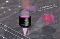
Professor Gu said by using a second donut-shaped beam to inhibit the photopolymerisation triggered by the writing beam in the donut ring, two-beam optical beam lithography can break the limit defined by the diffraction spot size of the two focused beams.
He said the key to 3D deep sub-diffraction optical beam lithography was the development with CSIRO of a unique two-photon absorption resin.
“This enabled a two-channel chemical reaction associated with the polymerisation and its counterpart of inhibited polymerisation, respectively, which eventually attributed to build mechanically robust nanostructures. Thus, the development of the vertical integration of integrated circuits, leading to ultra-fast optical information signal processors, becomes possible in the near future,” Professor Gu said.
The Latest Bing News on:
Petabyte storage
- Durham University Cosmologists, DiRAC and Dell Improve HPC Energy Efficiency without Sacrificing Performanceon May 1, 2024 at 5:01 am
SPONSORED GUEST ARTICLE] Since the beginning of human existence, people have looked into the night sky and wondered how the universe began. Cosmologists using the UK’s Memory Intensive DiRAC HPC ...
- Empowering enterprise growth: Resilient storage solutions in the age of accelerated computingon April 26, 2024 at 1:15 pm
Discussing resilient storage and the newly released FS5300 storage model, including its cyber resilience features, with IBM's Jim Comstock.
- Storage News - Page 1on April 25, 2024 at 7:21 pm
Spectra Logic has just announced their behemoth Spectra Cube, a modern tape storage library with a frankly insane 75PB of data capacity. 75 petabytes = 75,000 terabytes, or 75,000TB. Mammoth.
- Storage: A Secret to IoT Innovationon April 23, 2024 at 8:08 am
Here are three ways storage devices are evolving to meet the unique requirements in IoT in the field. The Internet of Things (IoT) continues to open up exciting opportunities for innovation. New ...
- AI News: Nigerian Government Debuts AI Tool with Multilingual Capabilitieson April 20, 2024 at 9:15 am
Nigeria launches a multilingual AI model, enhancing AI leadership in Africa with support from global tech giants and a $3.5M fund.
- AWS Snowmobile drives into the sunseton April 19, 2024 at 2:00 am
Customer demand for more efficient methods and faster online data transfer capabilities have led AWS to exit the data trucking business.
- Starfish Helps Tame the Wild West of Massive Unstructured Dataon April 18, 2024 at 3:34 pm
What data do you have? And can I access it?” Those may seem like simple questions for any data-driven enterprise. But when you have billions of files ...
- AWS retires Snowmobile truck-based data transfer serviceon April 17, 2024 at 8:37 am
Amazon Web Services (AWS) has ceased offering to transport data via an 18-wheeler truck after eight years. Announced in 2016 by bringing a semi-truck on stage, AWS Snowmobile was a 45 ft, 100 petabyte ...
- Spectra Logic Ups the Ante in Tape Storageon April 16, 2024 at 5:01 pm
scalable storage solutions with minimal operational impact, ensuring that business continuity is maintained even during upgrades and expansions. The Spectra Cube offers up to 30 petabytes of native ...
- The 50 Coolest Software-Defined Storage Vendors: The 2024 Storage 100on April 15, 2024 at 7:00 am
The company’s technology lets users monitor and manage data movement between its Myriad cloud-native scale-out file and object software for petabytes of flash storage or its StorNext shared ...
The Latest Google Headlines on:
Petabyte storage
[google_news title=”” keyword=”World Wide Web” num_posts=”10″ blurb_length=”0″ show_thumb=”left”]
The Latest Bing News on:
Optical computing
- SkyWater and Lumotive Announce Qualification and Production Start for World's First Commercially Available Optical Beamforming Chipon May 1, 2024 at 4:17 am
SkyWater Technology (NASDAQ: SKYT), the trusted technology realization partner, and Lumotive, a pioneer in optical semiconductor technology for 3D sensing, announced today that the companies have ...
- POET Announces Additional Private Placement Financing for CAD$10 Millionon April 29, 2024 at 2:40 pm
NOT FOR DISTRIBUTION TO U.S. NEWS WIRE SERVICES OR FOR DISSEMINATION IN THE UNITED STATESTORONTO, April 29, 2024 (GLOBE NEWSWIRE) -- POET ...
- Individual polyatomic molecules are trapped in optical-tweezer arrayson April 24, 2024 at 8:28 am
Individual polyatomic molecules have been trapped in arrays of optical tweezers for the first time. Researchers in the US were able to control individual quantum states of the three-atom molecules and ...
- AI Efficiency Breakthrough: How Sound Waves Are Revolutionizing Optical Neural Networkson April 23, 2024 at 12:34 pm
Researchers have developed a way to use sound waves in optical neural networks, enhancing their ability to process data with high speed and energy efficiency. Optical neural networks may provide the ...
- 2D materials rotate light polarizationon April 21, 2024 at 5:00 pm
Current integrated optical chips consist of only a few hundred elements on a chip. By comparison, a computer processor chip contains many billions of switching elements. The work of the German ...
- Study shows ultra-thin two-dimensional materials can rotate the polarization of visible lighton April 21, 2024 at 5:00 pm
Current integrated optical chips consist of only a few hundred elements on a chip. By comparison, a computer processor chip contains many billions of switching elements. The work of the German ...
- Compact quantum light processing: New findings lead to advances in optical quantum computingon April 19, 2024 at 11:00 am
An international collaboration of researchers, led by Philip Walther at University of Vienna, have achieved a significant breakthrough in quantum technology, with the successful demonstration of ...
- F5.5G All-Optical Premium Computing Network, Connecting Ubiquitous Intelligenceon April 17, 2024 at 7:57 am
Without doubt, the F5.5G all-optical premium computing network is the best option for carrying computing power, and it consists of three parts: First, 3D-mesh backbone computing network.
- F5.5G All-Optical Premium Computing Network, Connecting Ubiquitous Intelligenceon April 17, 2024 at 7:47 am
During the 21st Huawei Analyst Summit, the "Building F5.5G All-Optical Target Network, and Ushering in 10 Gbps UBB Intelligent Era" ...
The Latest Google Headlines on:
Optical computing
[google_news title=”” keyword=”optical computing” num_posts=”10″ blurb_length=”0″ show_thumb=”left”]

