Paves the road to much higher-performance servers, data centers and supercomputers in the years to come
In what is likley a significant development for the future of optical communications, IBM researchers have managed to shrink optical components to fit alongside their electrical counterparts on a single chip. This advance in the realm of “silicon nanophotonics” paves the road to much higher-performance servers, data centers and supercomputers in the years to come.
Having built about 200 of the world’s 500 fastest supercomputers to date, IBM is putting a great deal of effort into developing technology to raise the performance bar even higher. Besides, the competition isn’t exactly waiting around: China, India and the American company SGI have already announced plans to build supercomputers of their own with a performance approaching one exaflop – one billion billion floating point operations per second, a fifty-fold improvement over today’s fastest supercomputer – by as early as 2017.
The performance of microprocessors increases exponentially as years go by and yet, when it comes to putting together tens of thousands of them to create a supercomputer or a big data center, this doesn’t automatically translate into proportionally higher speeds. A system of this magnitude can only move as fast as the slowest of its components and, as it turns out, the main bottleneck here is the speed at which data can be sent across the different processors. The existing copper interconnects are limited in bandwidth and are expensive relative to their performance, costing several dollars per Gbit/s.
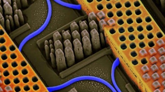
Ten years ago, IBM set its sights on solving the issue by pushing a technology that it dubbed “silicon nanophotonics.” The idea behind it is to increase the throughput of data communication between chips by switching from copper to optical signaling. In much the same way integrated circuits bundle an increasing number of transistors into a single die, IBM is shrinking optical componentry into far smaller and more powerful form factors.
As part of its research, IBM has now announced it has managed to shrink the optical components down to the 90 nm scale. This is of crucial importance, because it means that optical components can for the first time be built using the familiar, well-oiled manufacturing processes used to create electronics, and then embedded side by side with them on a single chip.
via Gizmag – Dario Borghino
The Latest Streaming News: Optical communications updated minute-by-minute
Bookmark this page and come back often
Latest NEWS
Latest VIDEO