


CREDIT
UCSB
A new transistor developed by UC Santa Barbara engineers overcomes one of the fundamental limitations of conventional transistors and reduces power dissipation by over 90 percent
One of the greatest challenges in the evolution of electronics has been to reduce power consumption during transistor switching operation. In a study recently reported in Nature, engineers at University of California, Santa Barbara, in collaboration with Rice University, have demonstrated a new transistor that switches at only 0.1 volts and reduces power dissipation by over 90% compared to state-of-the-art silicon transistors (MOSFETs).
MOSFETs have been the building blocks of everyday electronic products since the 1970s. However, to sustain the ever-growing need for increased transistor densities, miniaturization of MOSFETs has given rise to a power dissipation challenge due to the fundamental limitations of their turn-on characteristics.
“The steepness of a transistor’s turn-on is characterized by a parameter known as the subthreshold swing, which cannot be lowered below a certain level in MOSFETs,” explained Kaustav Banerjee, Professor of Electrical and Computer Engineering at UC Santa Barbara. A minimum gate voltage change of 60 millivolts at room temperature is required to change the current by a factor of ten in MOSFETs. In essence, the existing state of transistor technology limits the energy efficiency potential of digital circuits in general.
The research group of Professor Kaustav Banerjee at UC Santa Barbara took a new approach to subverting this fundamental limitation. They employed the quantum mechanical phenomenon of band-to-band tunneling to design a tunnel field effect transistor (TFET) with sub-60mV per decade of subthreshold swing.
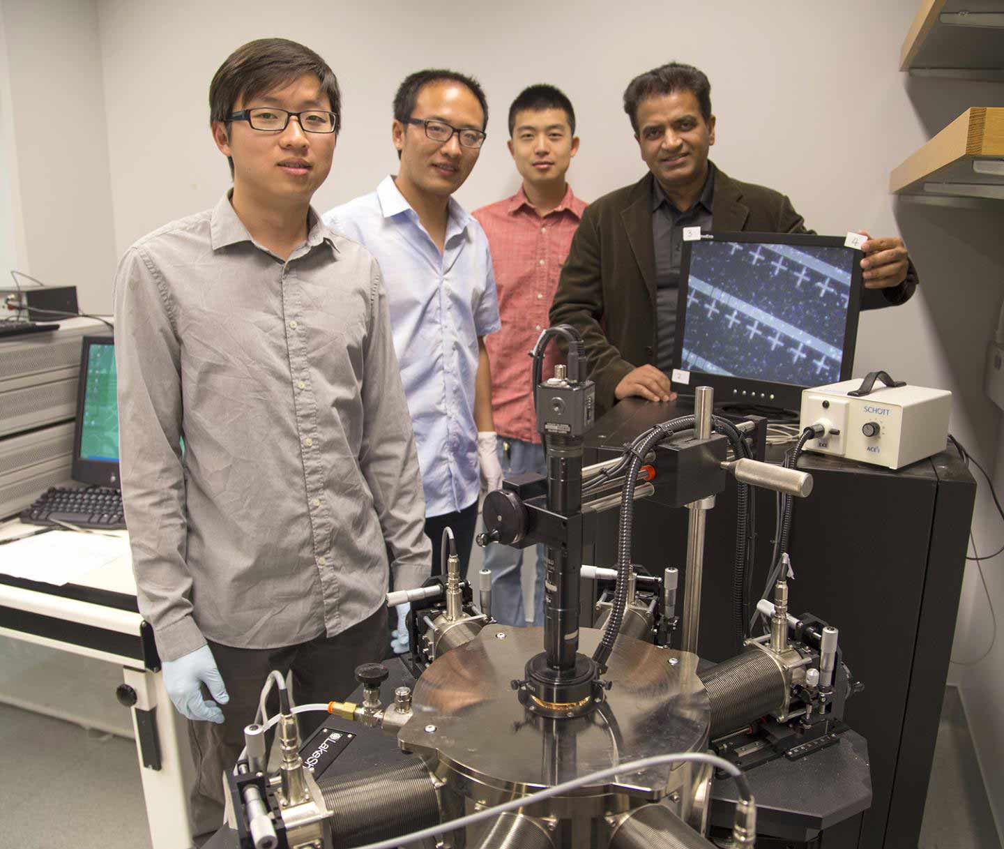
“We restructured the transistor’s source to channel junction to filter out high energy electrons that can diffuse over the source/channel barrier even in the off state, thereby making the off state current negligibly small,” explained Banerjee. At UCSB, Banerjee’s Nanoelectronics Research Lab includes Deblina Sarkar, Xuejun Xie, Wei Liu, Wei Cao, Jiahao Kang, and Stephan Kraemer, as well as Yongji Gong and Pulickel Ajayan of Rice University.
Banerjee and his colleagues are motivated by a global electronics industry that loses billions of dollars each year to the impact of power dissipation on chip cost and reliability. “This translates into lower battery lifetime in personal devices like cell phones and laptops, and massive power consumption of servers in large data centers,” adds Banerjee, pointing out the global scale of this energy demand.
An industry that relies on conventional semiconductors such as silicon or III-V compound semiconductors as the channel material for TFETs, Banerjee explains, “faces limitations because these materials have high density of surface states, which increase leakage current and degrade the subthreshold swing.”
The TFET designed by the UCSB team overcame this challenge in a few ways, most significant being the use of a layered two-dimensional (2D) material called molybdenum disulphide (MoS¬2). As the current-carrying channel placed over a highly doped germanium (Ge) as the source electrode, MoS2 offers an ideal surface and thickness of only 1.3nm. The resulting vertical heterostructure provides a unique source-channel junction that is strain-free, has a low barrier for current-carrying electrons to tunnel through from Ge to MoS¬2 through an ultra-thin (~0.34nm) van der Waals gap, and a large tunneling area.
“The crux of our idea is to combine 3D and 2D materials in a unique heterostructure, to achieve the best of both worlds. The matured doping technology of 3D structures is married to the ultra-thin nature and pristine interfaces of 2D layers to obtain an efficient quantum-mechanical tunneling barrier, which can be easily tuned by the gate,” commented Deblina Sarkar, lead author of the paper and PhD student in Banerjee’s lab.
“We have engineered what is, at present, the thinnest-channel subthermionic transistor ever made,” said Banerjee. Their atomically-thin and layered semiconducting channel tunnel FET (or ATLAS-TFET) is the only planar architecture TFET to achieve subthermionic subthreshold swing (~30 millivolts/decade at room temperature) over four decades of drain current, and the only one in any architecture to achieve so at an ultra-low drain-source voltage of 0.1V.
Ajayan, co-author and professor of chemical and biomolecular engineering at Rice University, commented, “This is a remarkable example showing the uniqueness of 2D atomic layered materials that enables device performance which conventional materials will not be able to achieve. This is perhaps the first breakthrough in a series of novel devices that people will now aspire to build using 2D materials.”
“The work is a significant step forward in the search for a low voltage logic transistor. The demonstration of sub-thermal operation over four orders of magnitude is impressive, and the on-current also advances the state-of-the-art. There is still a long ways to go, but this work demonstrates the potential of 2D materials to realize the long-sought, low-voltage device,” commented Mark Lundstrom, professor of electrical and computer engineering at Purdue University.
“We have demonstrated how to achieve the most important metric of steep subthreshold swing that meets ITRS requirements. Our transistor can be utilized for a number of low-power applications including arenas where the steep subthreshold swing is the main requirement, such as biosensors or gas sensors. With improved performance, the range of applications of this transistor can be further expanded,” explained Wei Cao, a PhD student in Banerjee’s group and a co-author of the article.
Read more: Atomically flat tunnel transistor overcomes fundamental power challenge of electronics

The Latest on: Tunnel transistor
[google_news title=”” keyword=”Tunnel transistor” num_posts=”10″ blurb_length=”0″ show_thumb=”left”]
via Google News
The Latest on: Tunnel transistor
- Million qubits chip a possibility, could enable practical quantum computerson May 7, 2024 at 5:28 am
The breakthrough opens the door to integrating millions of qubits on a single chip using mature manufacturing processes. For practical quantum computers to become a reality, breakthroughs like this ...
- Kaimai rail tunnel to get upgradeon May 4, 2024 at 5:00 pm
David Gordon (left) from Kiwirail, Simon Bridges and Todd McClay visit the Kaimai Tunnel. Photo / Andrew Warner New Zealand's longest train tunnel is set for a multimillion-dollar upgrade for the ...
- A Micro Light-Emitting Transistor With An N-Channel GaN FET In Series With A GaN LEDon May 1, 2024 at 5:00 pm
A technical paper titled “Tunnel Junction-Enabled Monolithically Integrated GaN Micro-Light Emitting Transistor” was published by researchers at the Ohio State University and Sandia National ...
- When does a conductor not conduct? Switching a 2D metal-organic framework from an insulator to a metalon April 29, 2024 at 7:40 am
An Australian-led study has found unusual insulating behavior in a new atomically-thin material—and the ability to switch it on and off.
- Quantum interference could lead to smaller, faster, and more energy-efficient transistorson March 25, 2024 at 10:45 am
An international team of researchers from Queen Mary University of London, the University of Oxford, Lancaster University, and the University of Waterloo have developed a new single-molecule ...
- Stephen Curry Says He Started Caring More About His Pregame 'Tunnel Walk' Looks Due to Social Media (Exclusive)on March 21, 2024 at 3:59 pm
"It's not just the two hours that we're on the court that people see us," Curry tells PEOPLE of using his platform to support Black designers Nathan Congleton/NBC/getty For Stephen Curry, the pre ...
- The emergence of spin electronics in data storageon December 9, 2023 at 6:09 pm
Electrons have a charge and a spin, but until recently these were considered separately. In classical electronics, charges are moved by electric fields to transmit information and are stored in a ...
- Transistors explained – what they are and what they doon October 24, 2022 at 11:53 am
The result was a chip with better performance, lower power consumption and a leading status through the 2010s. Tunnel field-effect transistors (TFETs) Tunnel field-effect transistors are a type of ...
- ELEC_ENG 401: Fundamentals of Electronic Deviceson November 8, 2019 at 6:35 pm
WEEK 7: Metal-oxide-semiconductor field-effect transistor (MOSFET):basic device characteristics, nonuniform doping and buried-channel devices, short-channel effects, MOSFET structures, nonvolatile ...
- Tunnel Diode/Transistor Differential Comparatoron February 21, 2018 at 6:09 am
A new tunnel diode/transistor circuit topology is reported, which both increases speed and reduces power in differential comparators. This circuit topology is of special interest for use in direct ...
via Bing News

