


Reduced costs for industry
A team of researchers from the Nanoengineering Research Centre (CRNE) and the Department of Electronic Engineering at the Universitat Politècnica de Catalunya · Barcelona Tech (UPCn has found a way to make the manufacture of crystalline silicon materials faster and more affordable. The results of their research have recently been published in the online version of the landmark journal Applied Physics Letters.
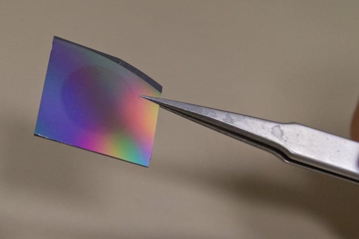
Thin crystalline silicon wafers measuring around 10 µm (micres) are costly but also very sought after in the field of microelectronics, especially in view of the growing demand for 3D circuit integration with microchips. Silicon wafers also have potential photovoltaic applications in the medium term in the conversion of sunlight to electricity and the production of more affordable, more flexible and lighter solar cells.
In recent years, techniques have been developed to obtain increasingly thinner crystalline silicon wafers from monocrystalline cylindrical ingots. Layers cut from the ingots using a multithreaded saw impregnated with abrasive material have a minimum thickness of around 150 µm. Obtaining wafers that are any thinner is more complicated, as existing methods only allow such wafers to be obtained one at a time. Furthermore, 50% of the silicon is lost in the process.
The technology developed by the research team – David Hernández, Trifon Trifonov and Moisés Garín, led by Professor Ramon Alcubilla – enables a large number of crystalline layers, controlled for thickness, to be produced from a single crystalline silicon wafer in just a single step. The outcome is a kind of crystalline silicon “millefeuille” produced more efficiently, more rapidly and more affordably than by existing methods.
The Latest Bing News on:
Thin crystalline silicon wafers
- Research team develops new thin film deposition process for tin selenide-based materialson May 9, 2024 at 6:45 am
This process utilizes the metal-organic chemical vapor deposition (MOCVD) method, enabling thin film deposition on large wafer surfaces at a low temperature of 200°C, achieving exceptional precision ...
- Heterojunction at the height of its poweron May 8, 2024 at 2:37 am
As it strives to increase performance while simultaneously reducing costs, Huasun has quickly moved from its first-generation heterojunction (HJT) cell to its current third- generation cell, and the ...
- The ‘magic’ of photovoltaic cellson April 29, 2024 at 5:00 pm
Solar panels are made up of many solar cells connected to form a grid of cells or an array. The most popular choice of material in these cells is silicon in the form of a crystalline structure.
- How Do Solar Panels Work?on April 26, 2024 at 5:00 pm
Similarly, crystalline silicon panels can withstand more abuse and weathering than some thin-film solar cells ... instead of using a rigid crystal wafer shot through with dopants, you vapor ...
- Indian imports of monocrystalline silicon wafers from China have surged, why?on April 16, 2024 at 5:01 pm
India almost doubled its imports of silicon wafers from China in 2023, highlighting India's expansion in solar cells and modules amid rising dependence on China's materials. According to the ...
- Switching to solar? We explain three main types of solar panelson April 13, 2024 at 1:31 pm
The silicon ingot is then sliced into thin wafers to make solar cells ... Generally less efficient than crystalline silicon panels Degradation is around 200% of what you’d get from other ...
- Thin Filmon February 10, 2021 at 5:51 pm
Today, silicon solar cells are still produced in almost equal shares from mono- and multi-crystalline silicon wafers. The authors here look at the scope for efficiencies in the wire sawing process ...
- Photovoltaic Device Teamon August 17, 2020 at 1:38 am
The use of thin crystalline silicon as a bottom cell provides high efficiency and ... 5】GaAs/Si-based three-junction smart stack cell Apparatus that etches a single side of the wafer by spin rotation.
- Wafer and Thin Film Instrumentation Informationon August 14, 2020 at 4:51 am
Wafer and thin film instrumentation consists of devices such as critical ... works on a similar principal to the SEM. They study surfaces of crystalline materials and gather data solely from a ...
- From Sand To Waferson April 17, 2019 at 5:00 pm
Silicon wafers are fundamental in manufacturing the ... in polycrystalline (“poly”) and amorphous (glass-like non-crystalline) forms is used in photovoltaic (solar) cells and thin film transistors.
The Latest Google Headlines on:
Thin crystalline silicon wafers
[google_news title=”” keyword=”thin crystalline silicon wafers” num_posts=”10″ blurb_length=”0″ show_thumb=”left”]
The Latest Bing News on:
Crystalline silicon materials
- 2D all-organic perovskites: potential use in 2D electronicson May 9, 2024 at 12:09 pm
Perovskites are among the most researched topics in materials science. Recently, a research team has solved an age-old challenge to synthesize all-organic two-dimensional perovskites, extending the ...
- PolyU researchers create 2D all-organic perovskites and demonstrate potential use in 2D electronicson May 9, 2024 at 7:04 am
These molecularly thin 2D organic perovskites are fundamentally different from traditional 3D minerals, they are single crystalline in two dimensions ... values surpass those of commonly used ...
- Heterojunction at the height of its poweron May 8, 2024 at 2:37 am
As it strives to increase performance while simultaneously reducing costs, Huasun has quickly moved from its first-generation heterojunction (HJT) cell to its current third- generation cell, and the ...
- Researchers create 2D all-organic perovskites, demonstrate potential use in 2D electronicson May 6, 2024 at 6:49 am
Perovskites are among the most researched topics in materials science. Recently, a research team from The Hong Kong Polytechnic University (PolyU) has solved an age-old challenge to synthesize ...
- The ‘magic’ of photovoltaic cellson April 29, 2024 at 5:00 pm
Solar panels are made up of many solar cells connected to form a grid of cells or an array. The most popular choice of material in these cells is silicon in the form of a crystalline structure.
- Crystalline Silicon PV Market Size, Share, Key Players, Revenue, Demand, and Forecast to 2024 to 2032on April 28, 2024 at 3:34 pm
Request To Download Free Sample of This Strategic Report @- The world crystalline silicon PV market is expected to grow at a CAGR of 11.3% during the forecast period. Crystalline silicon (c-Si) is one ...
- How Do Solar Panels Work?on April 26, 2024 at 5:00 pm
Tesla Solar Roof tiles use crystalline silicon cells. Credit: Tesla Crystalline silicon is often the material of choice for solar cells because of its durability. The windows on the space shuttles ...
- Imperial Academic Secures €2.4m European Funding to Enhance Solar Harvesting Technologyon April 26, 2024 at 4:40 pm
Professor Jenny Nelson has won a prestigious European Research Council grant to learn lessons from plants and apply them to solar technologies.She will use the grant to unpick how plants convert ...
- Fantastic plasticon April 20, 2024 at 2:33 am
Much of the early work on photoactive materials for photovoltaics focused on crystalline silicon, which dominates the commercial solar-energy field today. Several other materials, such as ...
- Novel Quantum Effect Observed in a Crystalline Materialon April 10, 2024 at 5:00 pm
Physicists have observed a novel quantum effect termed “hybrid topology” in a crystalline material ... Second, simple and elemental material systems (like silicon for conventional electronics) that ...
The Latest Google Headlines on:
Crystalline silicon materials
[google_news title=”” keyword=”crystalline silicon materials” num_posts=”10″ blurb_length=”0″ show_thumb=”left”]