


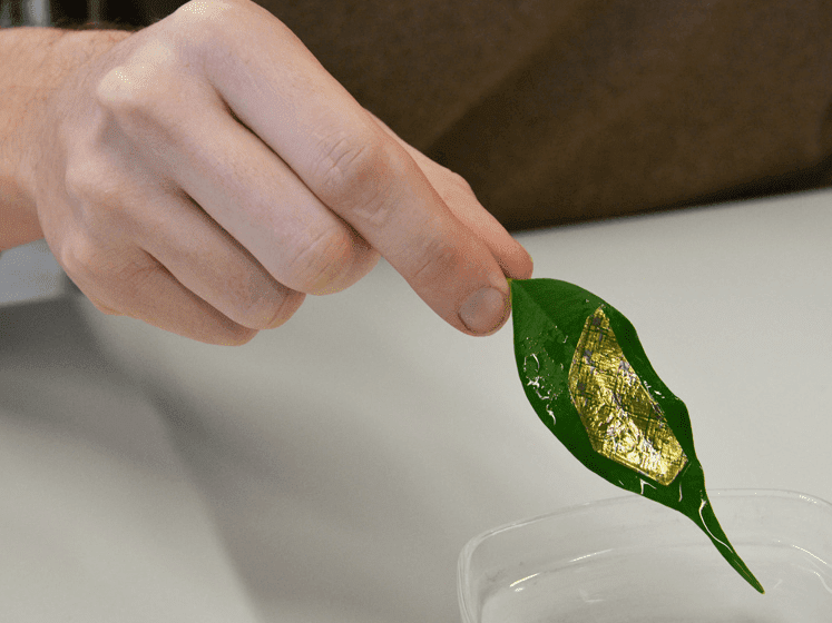
“These new thin-film transistors adhere to a wide range of surfaces and adapt perfectly”
Researchers at ETH are developing electronic components that are thinner and more flexible than before. They can even be wrapped around a single hair without damaging the electronics. This opens up new possibilities for ultra-thin, transparent sensors that are literally easy on the eye.
Niko Münzenrieder submerges a ficus leaf in water containing pieces of a shiny metallic membrane. Using tweezers, he carefully moves one of these pieces on to the leaf of the houseplant. On lifting the leaf, the film sticks to it like glue. The post-doctoral researcher is demonstrating the special characteristics of this electronic component in the form of an ultra-thin membrane, which he has helped to develop. “These new thin-film transistors adhere to a wide range of surfaces and adapt perfectly,” explains the physicist.
In Professor Gerhard Tröster’s Electronics Lab, scientists have been researching flexible electronic components, such as transistors and sensors, for some time now. The aim is to weave these types of components into textiles or apply them to the skin in order to make objects ‘smart’, or develop unobtrusive, comfortable sensors that can monitor various functions of the body.
Supple but functional
The researchers have now taken a big step towards this goal and their work has recently been published in the journal Nature Communications. With this new form of thin-film technology, they have created a very flexible and functional electronics.
Within a year, Münzenrieder, together with Giovanni Salvatore, has developed a procedure to fabricate these thin-film components. The membrane consists of the polymer parylene, which the researchers evaporate layer by layer into a conventional two-inch wafer. The parylene film has a maximum thickness of 0.001 mm, making it 50 times thinner than a human hair. In subsequent steps, they used standardised methods to build transistors and sensors from semiconductor materials, such as indium gallium zinc oxide, and conductors, such as gold. The researchers then released the parylene film with its attached electronic components from the wafer.
An electronic component fabricated in this way is extremely flexible, adaptable and – depending on the material used for the transistors – transparent. The researchers confirmed the theoretically determined bending radius of 50 micrometers during experiments in which they placed the electronic membrane on human hair and found that the membrane wrapped itself around the hair with perfect conformability. The transistors, which are less flexible than the substrate due to the ceramic materials used in their construction, still worked perfectly despite the strong bend.
Smart contact lens measures intraocular pressure
Münzenrieder and Salvatore see ‘smart’ contact lenses as a potential area of application for their flexible electronics. In the initial tests, the researchers attached the thin-film transistors, along with strain gauges, to standard contact lenses. They placed these on an artificial eye and were able to examine whether the membrane, and particularly the electronics, could withstand the bending radius of the eye and continue to function. The tests showed, in fact, that this type of smart contact lens could be used to measure intraocular pressure, a key risk factor in the development of glaucoma.
However, the researchers must still overcome a few technical obstacles before a commercially viable solution can be considered. For instance, the way in which the electronics are attached to the contact lens has to be optimised to take into account the effects of the aqueous ocular environment. In addition, sensors and transistors require energy, albeit only a small amount, which currently has to be provided from an external source. “In the lab, the film can be easily connected to the energy supply under a microscope. However, a different solution would need to be found for a unit attached to the actual eye,” says Münzenrieder.
Professor Tröster’s laboratory has already attracted attention in the past with some unusual ideas for wearable electronics. For example, the researchers have developed textiles with electronic components woven into them and they have also used sensors to monitor the bodily functions of Swiss ski jumping star Simon Ammann during his jumps.
The Latest on: Thin-film technology
[google_news title=”” keyword=”Thin-film technology” num_posts=”10″ blurb_length=”0″ show_thumb=”left”]
via Google News
The Latest on: Thin-film technology
- Construction begins on Gstar’s new factory in Jakartaon April 30, 2024 at 10:49 am
Gstar has announced the commencement of construction of its new silicon rod and silicon wafer factory in Jakarta, Indonesia. The factory, covering 60,000ft², is expected to feature fully digitalised ...
- Midsummer to build 200MW CIGS thin-film solar cell facility in Flen, Swedenon April 30, 2024 at 3:06 am
Swedish solar manufacturer Midsummer has selected the municipality of Flen in central Sweden to build a 200MW thin-film solar cell facility.
- South Korea plans 120 GW space solar projecton April 29, 2024 at 7:45 am
Two Korean research institutes are designing the 2.2 km × 2.7 km Korean Space Solar Power Satellite project with the aim of providing approximately 1 TWh of electricity to the Earth per year. The ...
- Thin Film Semiconductor Deposition Market Analysis, Key Segments, Share, Size, Growth Status, and Forecast to 2024 to 2032on April 28, 2024 at 3:35 pm
Report Ocean has recently unveiled its research findings on the “Thin Film Semiconductor Deposition Market” spanning from 2024 to 2032. This comprehensive report thoroughly analyzes the market ...
- New research demonstrates potential of thin-film electronics for flexible chip designon April 24, 2024 at 8:00 am
The mass production of conventional silicon chips relies on a successful business model with large "semiconductor fabrication plants" or "foundries." New research by KU Leuven and imec shows that this ...
- Opening up the potential of thin-film electronics for flexible chip designon April 23, 2024 at 5:00 pm
The mass production of conventional silicon chips relies on a successful business model with large 'semiconductor fabrication plants' or 'foundries'. New research by shows that this 'foundry' model ...
- First Solar and ZSW collaborate on thin-film PV techon April 22, 2024 at 6:30 am
Leading solar company First Solar and research institute ZSW have announced a partnership to develop new technology for thin film solar PV. Based in Stuttgart, Germany, ZSW is a research institute ...
- Global Thin Film Battery Market Report 2023-2028: A $2.5 Billion Opportunity, Driven by Demand in Electronics, Medical Devices, and IoT Applicationson April 19, 2024 at 7:31 am
The "Thin Film Battery Market - Global Industry Size, Share, Trends, Opportunity, and Forecast, 2018-2028F" report has been added to ResearchAndMarkets.com's offering. This comprehensive research into ...
- ZSW, First Solar partner to collaborate on thin-film PVon April 19, 2024 at 6:00 am
Württemberg (ZSW) and First Solar have agreed to work together to develop thin-film PV technologies on a gigawatt scale.
- Comprehensive model unravels quantum-mechanical effects behind photoluminescence in thin gold filmson April 19, 2024 at 5:32 am
EPFL researchers have developed the first comprehensive model of the quantum-mechanical effects behind photoluminescence in thin gold films; a discovery that could drive the development of solar fuels ...
via Bing News
