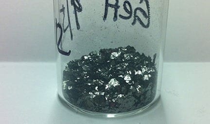
The element germanium in its natural state. Researchers at The Ohio State University have developed a technique for making one-atom-thick sheets of germanium for eventual use in electronics. Photo by Joshua Goldberger, courtesy of The Ohio State University.
Work could ultimately lead to electrical conductors that are 100 percent efficient
The future of electronics could lie in a material from its past, as researchers from The Ohio State University work to turn germanium—the material of 1940s transistors—into a potential replacement for silicon.
At the American Association for the Advancement of Science meeting, assistant professor of chemistry Joshua Goldberger reported progress in developing a form of germanium called germanane.
In 2013, Goldberger’s lab at Ohio State became the first to succeed at creating one-atom-thick sheet of germanane—a sheet so thin, it can be thought of as two-dimensional. Since then, he and his team have been tinkering with the atomic bonds across the top and bottom of the sheet, and creating hybrid versions of the material that incorporate other atoms such as tin.
The goal is to make a material that not only transmits electrons 10 times faster than silicon, but is also better at absorbing and emitting light—a key feature for the advancement of efficient LEDs and lasers.
“We’ve found that by tuning the nature of these bonds, we can tune the electronic structure of the material. We can increase or decrease the energy it absorbs,” Goldberger said. “So potentially we could make a material that traverses the entire electromagnetic spectrum, or absorbs different colors, depending on those bonds.”
As they create the various forms of germanane, the researchers are trying to exploit traditional silicon manufacturing methods as much as possible, to make any advancements easily adoptable by industry.
Aside from these traditional semiconductor applications, there have been numerous predictions that a tin version of the material could conduct electricity with 100 percent efficiency at room temperature.
Read more: The future of electronics—now in 2D
The Latest on: 2D electronics
[google_news title=”” keyword=”2D electronics” num_posts=”10″ blurb_length=”0″ show_thumb=”left”]
via Google News
The Latest on: 2D electronics
- Expert-Defying Anomaly – Scientists Discover 2D Nanomaterial With Counter-Intuitive Expanding Propertieson April 25, 2024 at 5:25 am
It is a common hack to stretch a balloon out to make it easier to inflate. When the balloon stretches, the width crosswise shrinks to the size of a string. Noah Stocek, a PhD student collaborating ...
- High-energy-density capacitors with 2D nanomaterials could significantly enhance energy storageon April 24, 2024 at 2:06 pm
In the quest for more efficient and sustainable energy solutions, a multi-university research team has reached a significant milestone in capacitor technology. Researchers from the University of ...
- New research demonstrates potential of thin-film electronics for flexible chip designon April 24, 2024 at 8:00 am
The mass production of conventional silicon chips relies on a successful business model with large "semiconductor fabrication plants" or "foundries." New research by KU Leuven and imec shows that this ...
- Scientists Create New 2D Form of Gold Called Goldeneon April 23, 2024 at 10:00 am
Since then, hundreds of 2D materials have been identified, most of which were much harder to isolate than graphene, but 2D metals are particularly tricky. Metal atoms tend to cluster together, forming ...
- Scientists stencil-paint carbon nanotube components for flexible transparent electronicson April 23, 2024 at 9:23 am
Researchers from Skoltech, MIPT, and elsewhere have found a fast and inexpensive way to create geometric patterns in carbon nanotube films. The resulting films turned out to have superior properties ...
- Novel material supercharges innovation in electrostatic energy storageon April 18, 2024 at 11:00 am
Electrostatic capacitors play a crucial role in modern electronics. They enable ultrafast charging and discharging, providing energy storage and power for devices ranging from smartphones, laptops and ...
- Novel material supercharges innovation in electrostatic energy storageon April 17, 2024 at 5:00 pm
The 2D/3D/2D heterostructures are finely crafted ... As the world grapples with the imperative of transitioning toward next-generation electronics components, Bae's novel heterostructure material ...
- Atom-by-atom: Imaging structural transformations in 2D materialson April 17, 2024 at 2:36 pm
Silicon-based electronics are approaching their physical limitations and new materials are needed to keep up with current technological demands. Two-dimensional (2D) materials have a rich array of ...
- Atom-by-atom: Imaging structural transformations in 2D materialson April 17, 2024 at 2:09 pm
Annular dark field scanning electron microscopy images of a bilayer interface after heat pulses at 500° (left), 600° (middle) and 700° (right). Dashed colored lines mark the positions of the ...
- Goldene: New 2D form of gold makes graphene look boringon April 16, 2024 at 8:46 pm
Graphene is a bit like the Novak Djokovic of materials – it’s so damn talented that each new achievement feels passé. But now, an exciting new upstart is challenging graphene’s title. Meet goldene, a ...
via Bing News


