


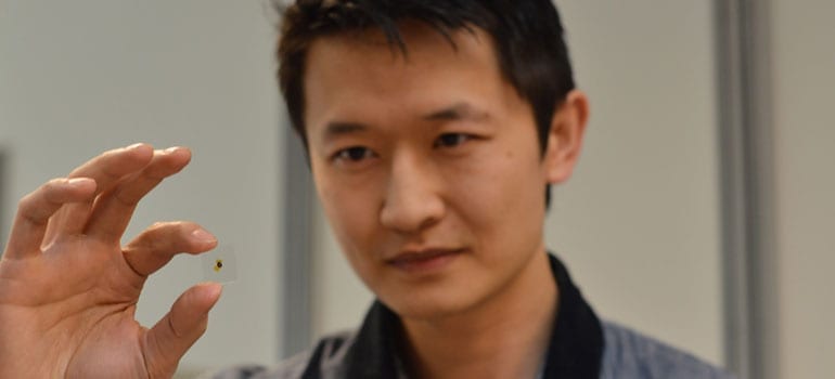
Physicists at the Technical University of Munich (TUM) have developed a nanolaser, a thousand times thinner than a human hair. Thanks to an ingenious process, the nanowire lasers grow right on a silicon chip, making it possible to produce high-performance photonic components cost-effectively. This will pave the way for fast and efficient data processing with light in the future.
Ever smaller, ever faster, ever cheaper – since the start of the computer age the performance of processors has doubled on average every 18 months. 50 years ago already, Intel co-founder Gordon E. Moore prognosticated this astonishing growth in performance. And Moore’s law seems to hold true to this day.
But the miniaturization of electronics is now reaching its physical limits. “Today already, transistors are merely a few nanometers in size. Further reductions are horrendously expensive,” says Professor Jonathan Finley, Director of the Walter Schottky Institute at TUM. “Improving performance is achievable only by replacing electrons with photons, i.e. particles of light.”
Photonics – the silver bullet of miniaturization
Data transmission and processing with light has the potential of breaking the barriers of current electronics. In fact, the first silicon-based photonics chips already exist. However, the sources of light for the transmission of data must be attached to the silicon in complicated and elaborate manufacturing processes. Researchers around the world are thus searching for alternative approaches.
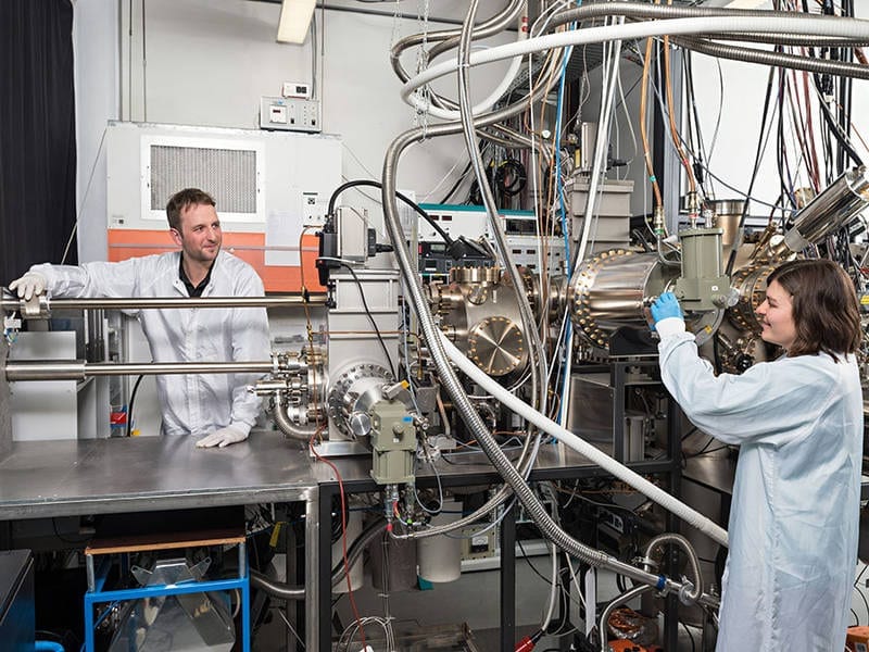
Scientists at the TU Munich have now succeeded in this endeavor: Dr. Gregor Koblmüller at the Department of Semiconductor Quantum-Nanosystems has, in collaboration with Jonathan Finley, developed a process to deposit nanolasers directly onto silicon chips. A patent for the technology is pending.
Growing a III-V semiconductor onto silicon requires tenacious experimentation. “The two materials have different lattice parameters and different coefficients of thermal expansion. This leads to strain,” explains Koblmüller. “For example, conventional planar growth of gallium arsenide onto a silicon surface results therefore in a large number of defects.”
The TUM team solved this problem in an ingenious way: By depositing nanowires that are freestanding on silicon their footprints are merely a few square nanometers. The scientists could thus preclude the emerging of defects in the GaAs material.
Atom by atom to a nanowire
But how do you turn a nanowire into a vertical-cavity laser? To generate coherent light, photons must be reflected at the top and bottom ends of the wire, thereby amplifying the light until it reaches the desired threshold for lasing.
To fulfil these conditions, the researchers had to develop a simple, yet sophisticated solution: “The interface between gallium arsenide and silicon does not reflect light sufficiently. We thus built in an additional mirror – a 200 nanometer thick silicon oxide layer that we evaporated onto the silicon,” explains Benedikt Mayer, doctoral candidate in the team led by Koblmüller and Finley. “Tiny holes can then be etched into the mirror layer. Using epitaxy, the semiconductor nanowires can then be grown atom for atom out of these holes.”
Only once the wires protrude beyond the mirror surface they may grow laterally – until the semiconductor is thick enough to allow photons to jet back and forth to allow stimulated emission and lasing. “This process is very elegant because it allows us to position the nanowire lasers directly also onto waveguides in the silicon chip,” says Koblmüller.
Basic research on the path to applications
Currently, the new gallium arsenide nanowire lasers produce infrared light at a predefined wavelength and under pulsed excitation. “In the future we want to modify the emission wavelength and other laser parameters to better control temperature stability and light propagation under continuous excitation within the silicon chips,” adds Finley.
The team has just published its first successes in this direction. And they have set their sights firmly on their next goal: “We want to create an electric interface so that we can operate the nanowires under electrical injection instead of relying on external lasers,” explains Koblmüller.
“The work is an important prerequisite for the development of high-performance optical components in future computers,” sums up Finley. “We were able to demonstrate that manufacturing silicon chips with integrated nanowire lasers is possible.”

Learn more: Nanolaser for information technology
The Latest on: Silicon chip with integrated laser
[google_news title=”” keyword=”Silicon chip with integrated laser” num_posts=”10″ blurb_length=”0″ show_thumb=”left”]
via Google News
The Latest on: Silicon chip with integrated laser
- Silicon Laboratories Inc. (NASDAQ:SLAB) Q1 2024 Earnings Call Transcripton April 25, 2024 at 8:09 am
April 24, 2024 Silicon Laboratories Inc. misses on earnings expectations. Reported EPS is $-1.77142 EPS, expectations were $-0.98. SLAB isn't one of the 30 most popular stocks among hedge funds at the ...
- SkyWater Technology Is Lowering Barriers To Advanced Chip Packagingon April 23, 2024 at 3:00 am
SkyWater has partnered with Deca Technologies to develop a multi chip packaging capability that will lower the entry barriers to advanced packaging.
- Silicon Creations Reaches Milestone of 10 Million Wafers in Production with TSMCon April 22, 2024 at 8:34 am
Silicon Creations, a leading supplier of high-performance analog and mixed-signal intellectual property (IP), announced a significant milestone: surpassing 10 million wafers in production containing ...
- Fraunhofer inverter project boosts EV performanceon April 21, 2024 at 11:06 am
Fraunhofer IZM is working with project partners Porsche and Bosch, in a project called Dauerpower, to develop an electric inverter that can work at a lower operating temperature thanks to optimised ...
- Intel completes assembly of world’s most advanced EUV lithography systemon April 19, 2024 at 10:07 am
Intel Corp.’s newly formed chip foundry business said today it has achieved a crucial milestone for the chipmaking industry by completing the assembly of the world’s first commercial High Numerical ...
- CS International champions a green agendaon April 19, 2024 at 7:12 am
Compound Semiconductor™ is an Angel Business Communications publication.
- Quantum computing, AI, and semiconductor innovationson April 18, 2024 at 8:02 am
In the dynamic landscape of technology, quantum computing and artificial intelligence (AI) emerge as transformative forces, poised to revolutionize industries and reshape investment paradigms.
- SK hynix signs Advanced Chip Packaging agreementon April 13, 2024 at 12:09 am
SK hynix will invest an estimated $3.87 billion in West Lafayette, Indiana to build an advanced packaging fabrication and R&D facility for AI products. The project, the first of its kind in the United ...
- Revolutionizing Microwave Signal Generation Breakthrough Photonic Chip Paves the Way for Compact, Low-Noise Deviceson March 21, 2024 at 1:13 am
In a groundbreaking achievement, researchers at Columbia Engineering have developed a revolutionary photonic chip capable of producing high-quality, ultra-low-noise microwave signals using only a ...
- Mycronic receives order for SLX mask writeron December 8, 2023 at 6:56 am
“We have now surpassed 50 orders since we launched the SLX at the end of 2019. This success has been driven by orders from new customers, as in this case, as well as repeat orders from semiconductor ...
via Bing News
