“This technique allows you to achieve ‘theoretical density,’ meaning it eliminates all of the porosity in the material”
A researcher from North Carolina State University has developed a technique for creating high-density ceramic materials that requires far lower temperatures than current techniques – and takes less than a second, as opposed to hours. Ceramics are used in a wide variety of technologies, including body armor, fuel cells, spark plugs, nuclear rods and superconductors.
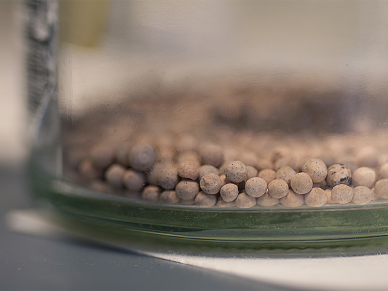
At issue is a process known as “sintering,” which is when ceramic powders (such as zirconia) are compressed into a desired shape and exposed to high heat until the powder particles are bound together into a solid, but slightly porous, material. But new research from Dr. Jay Narayan, John C. Fan Distinguished Chair Professor of Materials Science and Engineering at NC State, may revolutionize the sintering process.
Narayan’s new technique, selective-melt sintering, allows sintering of yttria-stabilized zirconia at 800 degrees Celsius (C) – instead of the conventional 1450 C. In addition, using the selective-melt sintering technique, it is possible to sinter zirconia at 800 C in less than a second, and create a material with no porosity at all. In contrast, traditional sintering techniques take four to five hours at 1450 C.
“This technique allows you to achieve ‘theoretical density,’ meaning it eliminates all of the porosity in the material,” Narayan says. “This increases the strength of the ceramic, as well as improving its optical, magnetic and other properties.”
The key to Narayan’s approach is the application of an electric field, at approximately 100 volts per centimeter, to the material. When this field is applied, it creates subtle changes in the material’s “grain boundaries” – where atoms from different crystals meet in the material. Namely, the field draws “defects” to the grain boundary. These defects consist of vacancies (missing atoms) which can carry charges. The defects are negatively charged and draw current from the electric field to the area – which raises the temperature along the grain boundary.
The Latest Bing News on:
High-Density Ceramics
- A centuries-old Japanese ceramics maker has found itself at the center of the AI revolutionon April 27, 2024 at 3:53 am
Maruwa, which builds ceramics for circuit boards and semiconductors, has seen its shares double over the past year, according to the Financial Times. And since April, its shares have been at an ...
- Ceramics centeron April 27, 2024 at 3:10 am
Shanxi connects the east with the west of China, making it a place where different ethnic groups and cultures meet. The ancient porcelain pieces discovered in Shanxi reflect the province's unique ...
- MAX Power Makes High-Grade Lithium Discovery at Arizona’s Willcox Playaon April 26, 2024 at 6:59 am
MAX Power Mining Corp. (CSE: MAXX; OTC: MAXXF; FRANKFURT: 89N) (“MAX Power” or the “Company”) is pleased to confirm the discovery of near-surface lithium-rich clays over a broad area of state-leased ...
- Researchers produce thinnest sheet of metal ever using a 100-year old Japanese technique — Goldene could pave way for super catalysts, ultra high density optical storage and ...on April 25, 2024 at 9:31 pm
Shun Kashiwaya, a researcher at the Materials Design Division at LiU, explains, "If you make a material extremely thin, something extraordinary happens. As with Graphene, the same thing happens with ...
- The 6 Best Plastic Cutting Boards, According to Our Expertson April 25, 2024 at 3:00 pm
While cutting boards are available in many materials, including wood, glass and ceramic, we’ve focused on plastic for ... Hayate Yoshihiro Hi-Soft High-Performance Professional Grade Cutting Board ...
- Towards novel promising perovskite-type ferroelectric materials: High-pressure synthesis of rubidium niobateon April 25, 2024 at 1:37 pm
Capacitors are crucial components in electronic devices such as smartphones and computers. They are made of dielectric materials that polarize on the application of the voltage. Currently, barium ...
- Preventing thermal runaway at every level of EV battery assemblyon April 21, 2024 at 3:07 am
There is currently a lack of clear regulation around TRP standards. But across the industry, many OEMs have adopted the “5-minute rule” as the standard, meaning if a thermal runaway event happens, ...
- This must be Topanga Canyonon April 19, 2024 at 3:00 am
After a particularly rainy season, multiple mudslides have blocked Topanga Canyon’s entry from PCH for more than a month. Shops, restaurants and other businesses that depend on visitors are struggling ...
- The 37 best gifts for coffee loverson April 18, 2024 at 12:24 pm
We found the best gifts for coffee lovers at every experience level and at nearly every price point — here’s what to buy, according to coffee experts and baristas.
- The 20 Best Pet Products on Amazon For Cleaning, Feeding, and Groomingon April 16, 2024 at 7:44 pm
Shop the best selling pet products and brands on Amazon, from accessories for your furry friend to cleaning products that help remove cat or dog hair.
The Latest Google Headlines on:
High-Density Ceramics
[google_news title=”” keyword=”High-Density Ceramics” num_posts=”10″ blurb_length=”0″ show_thumb=”left”] [/vc_column_text]The Latest Bing News on:
Sintering
- Colorado ski town company hopes to bring new sustainable vision to sports performance eyewearon April 27, 2024 at 9:37 am
Groundbreaking is the word that Jason Aronson, one of the founders of Zirkel Optics, likes to use when describing the new eyewear company, rooted in sustainability and cutting-edge technology, that ...
- Firmware update delivers high-definition capabilities to Stratasys Selective Absorption Fusion technologyon April 26, 2024 at 7:01 am
The new HighDef Printing capabilities have been designed to allow for exact and high-definition printing with detailed resolution using Stratasys' Selective Absorption Fusion (SAF) technology.
- Towards novel promising perovskite-type ferroelectric materials: High-pressure synthesis of rubidium niobateon April 25, 2024 at 1:37 pm
Capacitors are crucial components in electronic devices such as smartphones and computers. They are made of dielectric materials that polarize on the application of the voltage. Currently, barium ...
- NSL Analytical’s Delta Qualification to speed up Additive Manufacturing parts productionon April 25, 2024 at 4:57 am
The qualification of materials used in Additive Manufacturing is a thorough process, explains NSL Analytical Services.
- CADchat launches digital workspaces to aid product developmenton April 25, 2024 at 4:39 am
CADchat has launched its cloud-based digital workspace, offers tools intended to extend the functionality of traditional video calls.
- Companies donating the most money to Donald Trumpon April 23, 2024 at 1:19 am
Stacker examined data from OpenSecrets to see which companies are donating the most money to Donald Trump's 2024 presidential campaign.
- Redefining Space Construction: How Lunar Regolith Is Transforming Habitat Designon April 23, 2024 at 12:06 am
Scientists conducted a quantitative evaluation of techniques for solidifying and forming lunar regolith. As lunar missions transition from exploration to building and using structures, constructing on ...
- Where Fun Meets Functionalityon April 19, 2024 at 12:50 pm
At SCU, mechanical engineer Kira Hofelmann ’24 solves real-world robotic problems—and makes lightsabers in her spare time.
- Researchers quantify the ideal in situ construction method for lunar habitatson April 18, 2024 at 12:28 pm
As the lunar exploration mission evolves from exploration to construction and utilization, in situ lunar construction becomes an imperative requirement. The key is regolith solidification and ...
- MUSE: The First Star Stellarator With A 3D Printed Casingon April 18, 2024 at 7:00 am
Researchers at the Princeton Plasma Physics Laboratory (PPPL) have pooled their expertise to create a new type of stellarator generator with permanent magnets and a novel 3D printed housing. MUSE, as ...
The Latest Google Headlines on:
Sintering
[google_news title=”” keyword=”sintering” num_posts=”10″ blurb_length=”0″ show_thumb=”left”]

