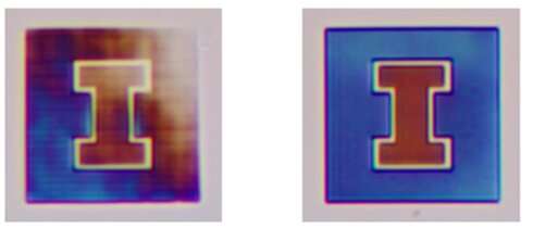
A line grating fabricated with SCRIBE to form the UIUC “I” logo with accurate colors. The left grating was fabricated without the improvements, and the right grating incorporates the improvements.
CREDIT: The Grainger College of Engineering at the University of Illinois Urbana-Champaign
3D printers form objects by layering melted plastic or metal, but this only works on large scales. What you need to fabricate microdevices for which the layering step is not feasible? What if it were possible to print directly into the bulk of an existing three-dimensional material?
The research groups of Lynford Goddard and Paul Braun, professors at the University of Illinois Urbana-Champaign, have been collaborating to develop such a process. They use the technique of multiphoton lithography to print inside an existing porous material with high intensity laser light. This allows the researchers to selectively modify regions of the interior and manufacture custom small-scale optical devices in a procedure called subsurface controllable refractive index via beam exposure, or SCRIBE. The two research groups recently announced a refinement to this procedure that gives them significantly tighter control over the resulting devices. The new procedure was recently published in ACS Photonics.
“We were able to show an improvement from a baseline of 36% to a new value of 49% in the efficiency of fabricated lenses and a clear improvement in the color uniformity resulting from the 2D line gratings we made,” said Alexander Littlefield, a graduate student in Goddard’s group and the study’s lead author. “We believe that this new technique will open the door to a vast array of optical element designs.”
SCRIBE is a form of multiphoton lithography that depends on a mechanism called two-photon absorption. The researchers use silicon that has been etched to have microscopic pores and oxidized into transparent silica. They then fill it with a material called photoresist, which can undergo a chemical process by which it changes its optical properties only when it absorbs two photons simultaneously—a process that is quite rare unless very intense light is used. The researchers take advantage of this by focusing laser light to create high intensities only in specific regions. This allows them to create custom designs for the material’s optical properties in three dimensions to “write” optical components.
Past versions of SCRIBE were limited by imperfect control of the laser’s intensity. To address this, the researchers present three improvements to the technique in their article. First, they use a two-photon fluorescence imaging system to map the photoresist’s density and correct the laser power needed for the desired result. Second, they smooth out errors that are especially prominent near the writing boundary by modulating the material’s position as the laser writes. Finally, they introduce a time delay between laser exposures to minimize time-dependent effects in the photoresist interaction.
By incorporating these three improvements, the researchers achieved tighter control over their patterned devices, achieving more precisely fabricated components that are much more effective. To demonstrate the versatility of their method, they fabricated a 100-by-100-micrometer optical device that alters light to form specific color patterns, a line grating, that reproduces the shape and colors of the UIUC logo (see figure).
“Our work shows that multiphoton lithography can now accurately fabricate microscale optical components with new capabilities that do not yet exist for other fabrication methods,” Goddard said.
Original Article: New procedure allows micro-printing inside existing materials with greater accuracy
More from: University of Illinois at Urbana Champaign
The Latest Updates from Bing News
Go deeper with Bing News on:
Multiphoton lithography
- Here’s Everything You Need To Know About Immersion Lithography
In semiconductor manufacturing, immersion lithography creates smaller and more intricate features on wafers. It enhances the resolution and precision of the lithography process. Immersion ...
- MAPPER and TSMC Take Next Step in Exploring Multiple E-beam Lithography for IC Manufacturing at 22 nanometer node and Beyond
Delft, The Netherlands / Hsinchu, Taiwan -- Ocotober 13, 2008 -- MAPPER Lithography and Taiwan Semiconductor Manufacturing Company (TSMC) signed an agreement, according to which MAPPER will ship its ...
- Here’s Everything You Need To Know About Lithography
In semiconductor manufacturing, lithography is a critical process that uses light to transfer intricate circuit (IC) patterns onto a silicon wafer. This process enables the creation of tiny ...
- Semiconductor Giant ASML Has a New Boss, and a Big Problem
“I have worked with Christophe for years, and look forward to continuing our great relationship as we deliver leading-edge lithography solutions,” says Ryan Russell, corporate vice president ...
- Intel finishes assembly of ASML's first High-NA EUV tool, ready for Intel 14A process in 2025
ASML provided Intel, its first customer, with the $380 million Twinscan EXE:5000 High-NA lithography machine. Yesterday, it shipped its second High-NA EUV lithography machine to a mystery customer.
Go deeper with Bing News on:
Microscale optical components
- optical mouse
If your pointing device is a mouse, turn it over. The chances are you’ll see a red LED light if you’re not seriously old-school and your mouse has a ball, this light serves as the illumination ...
- Scientists stencil-paint carbon nanotube components for flexible transparent electronics
Researchers from Skoltech, MIPT, and elsewhere have found a fast and inexpensive way to create geometric patterns in carbon nanotube films. The resulting films turned out to have superior properties ...
- 3D printed microscale synthetic brochosome (IMAGE)
Pictured is an array of 3D printed microscale synthetic brochosome ... studied the relationship between the optical properties and the geometric designs of the brochosomes utilizing 3D printed ...
- Revolutionizing Microscale 3D Printing Stanford’s Breakthrough Technique
Led by a team of visionaries at the DeSimone lab, this high-speed microscale 3D printing method represents a significant leap forward in precision engineering and opens up a multitude of ...
- Optical Guitar Pickup Works With Nylon Strings
So what do you do? You follow [Simon]’s example, and build an optical pickup instead. The concept is simple. You place an LED and a phototransistor in a U-shaped channel, and place it so that ...

