Cameras fitted with a new revolutionary sensor will soon be able to take clear and sharp photos in dim conditions, thanks to a new image sensor invented at Nanyang Technological University (NTU).
The new sensor made from graphene, is believed to be the first to be able to detect broad spectrum light, from the visible to mid-infrared, with high photoresponse or sensitivity. This means it is suitable for use in all types of cameras, including infrared cameras, traffic speed cameras, satellite imaging and more.
Not only is the graphene sensor 1,000 times more sensitive to light than current low-cost imaging sensors found in today’s compact cameras, it also uses 10 times less energy as it operates at lower voltages. When mass produced, graphene sensors are estimated to cost at least five times cheaper.
Graphene is a million times smaller than the thickest human hair (only one-atom thick) and is made of pure carbon atoms arranged in a honeycomb structure. It is known to have a high electrical conductivity among other properties such as durability and flexibility.
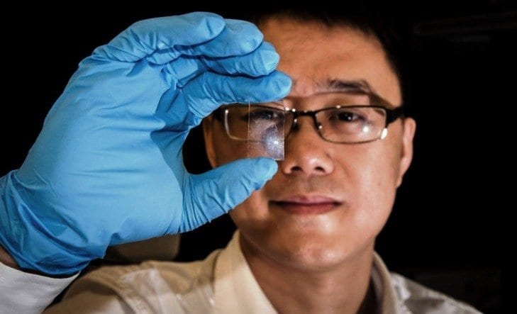
The inventor of the graphene sensor, Assistant Professor Wang Qijie, from NTU’s School of Electrical & Electronic Engineering, said it is believed to be the first time that a broad-spectrum, high photosensitive sensor has been developed using pure graphene.
His breakthrough, made by fabricating a graphene sheet into novel nano structures, was published this month in Nature Communications, a highly-rated research journal.
“We have shown that it is now possible to create cheap, sensitive and flexible photo sensors from graphene alone. We expect our innovation will have great impact not only on the consumer imaging industry, but also in satellite imaging and communication industries, as well as the mid-infrared applications,” said Asst Prof Wang, who also holds a joint appointment in NTU’s School of Physical and Mathematical Sciences.
“While designing this sensor, we have kept current manufacturing practices in mind. This means the industry can in principle continue producing camera sensors using the CMOS (complementary metal-oxide-semiconductor) process, which is the prevailing technology used by the majority of factories in the electronics industry. Therefore manufacturers can easily replace the current base material of photo sensors with our new nano-structured graphene material.”
If adopted by industry, Asst Prof Wang expects that cost of manufacturing imaging sensors to fall – eventually leading to cheaper cameras with longer battery life.
How the Graphene nanostructure works
Asst Prof Wang came up with an innovative idea to create nanostructures on graphene which will “trap” light-generated electron particles for a much longer time, resulting in a much stronger electric signal. Such electric signals can then be processed into an image, such as a photograph captured by a digital camera.
The “trapped electrons” is the key to achieving high photoresponse in graphene, which makes it far more effective than the normal CMOS or CCD (charge-coupled device) image sensors, said Asst Prof Wang. Essentially, the stronger the electric signals generated, the clearer and sharper the photos.
“The performance of our graphene sensor can be further improved, such as the response speed, through nanostructure engineering of graphene, and preliminary results already verified the feasibility of our concept,” Asst Prof Wang added.
The Latest Bing News on:
Graphene sensor
- Graphene in Biomedicine: Opportunities and Challengeson April 27, 2024 at 5:00 pm
Graphene, whose discovery won the 2010 Nobel Prize in physics, has been a shining star in the material science in the past few years. Owing to its interesting electrical, optical, mechanical and ...
- Thermal properties of new 2D materials for microchips can now be measured wellon April 18, 2024 at 8:09 am
Making ever smaller and more powerful chips requires new ultrathin materials: 2D materials that are only 1 atom thick, or even just a couple of atoms. Think about graphene or ultra-thin silicon ...
- Paragraf provides access to its graphene technology via new online storeon April 15, 2024 at 4:00 am
Paragraf, the UK-based mass producer of graphene electronics using transfer-free graphene grown with conventional semiconductor processes, has opened a new online store to enable global access to its ...
- Wafer-thin, stretchy and strong as steel: could ‘miracle’ material graphene finally transform our world?on April 13, 2024 at 9:26 am
“We used some of the first graphene we manufactured this way to make a sensor which can detect magnetic fields,” said Humphreys, who has since set up a spin-off company, Paragraf, with his team. Based ...
- Advancing biomedical diagnostics: Graphene sensor inks pave the way for precision biosensingon April 10, 2024 at 5:00 pm
Haydale began working with Cardiff University in 2021, specifically the Wales Kidney Research Unit (WKRU), to create a prototype biosensor using its functionalised biomedical sensor inks.
- Improving sodium ion batteries with mechanically robust nanocellular grapheneon April 7, 2024 at 5:00 pm
Graphene comprises two-dimensional sheets of ... to improve the performance of electronic devices, energy devices and sensors. But its development has been stymied by defects that occur during ...
- A bioelectronic mesh capable of growing with cardiac tissues for comprehensive heart monitoringon March 21, 2024 at 9:07 am
However, because CMT is grown in a test tube, it has to mature, a process that takes time and can be easily disrupted by a clumsy sensor. The second critical component involves graphene—a pure ...
The Latest Google Headlines on:
Graphene sensor
[google_news title=”” keyword=”graphene sensor” num_posts=”10″ blurb_length=”0″ show_thumb=”left”]
The Latest Bing News on:
Imaging sensors
- How do fingerprint sensors work?on April 24, 2024 at 5:00 pm
These scanners leverage visible light and an image capture device to record fingerprints ... As a finger presses against the sensor, the ridges affect the capacitor differently than the valleys ...
- What is BlueImage imaging technology that may launch with Vivo X100 Ultraon April 24, 2024 at 8:44 am
Vivo introduces BlueImage imaging tech in X100 series with Zeiss partnership. X100 Ultra rumored to feature 200 MP sensor, Snapdragon 8 Gen 3, 5,000mA ...
- Huawei Mate 70 series to feature China-developed image sensors for its main camerason April 23, 2024 at 2:00 am
Tech blogger Digital Chat Station revealed on Chinese social media platform Weibo yesterday that Huawei’s next-gen flagship Mate 70 series smartphones ...
- Moment T-series review: premium build quality but limited image gainson April 22, 2024 at 7:07 am
Moment's T-series lenses are well-built, offering the look and feel of a premium product. But with high-end smartphone cameras getting so good, can they still up your photo game? We decided to find ...
- Organic CMOS Image Sensor Market Segmentation Synergy Strategies for Identifying and Targeting Your Market Effectivelyon April 21, 2024 at 10:10 pm
Request To Download Free Sample of This Strategic Report @- Organic CMOS image sensor technology uses organic photoelectric conversion layer with high absorption coefficient, providing wider incident ...
- Organic CMOS Image Sensor Market Size Explorer’s Journey into Growth Navigationon April 21, 2024 at 2:06 pm
Report Ocean recently added a research report on “Organic CMOS Image Sensor Market”. The report includes an extensive analysis of the market’s characteristics, COVID-19 impact, size and growth, ...
- Studying optimization for neuromorphic imaging and digital twinson April 20, 2024 at 1:28 am
Science X is a network of high quality websites with most complete and comprehensive daily coverage of the full sweep of science, technology, and medicine news ...
- Researchers develop display screens with biometric sensor capabilitieson April 19, 2024 at 10:54 am
Traditional display screens like those built into smartphones require extra sensors for touch control, ambient light, and fingerprint sensing.
- Sony’s Starvis 2 Sensor available in IDS NXT Malibu for superior low-light imagingon April 19, 2024 at 1:04 am
IDS expands its product line for intelligent image processing and launches a new IDS NXT Malibu camera. It enables AI-based image processing, video compression, and streaming in full 4K ...
- CMOS Image Sensorson April 18, 2024 at 11:31 am
The Emerald Gen2 is the newest addition to Teledyne’s CMOS image sensor family. Emerald Gen2 is available in 8.9-megapixels or 12-megapixels, in monochrome or color, and in two-speed grades, standard ...
The Latest Google Headlines on:
Imaging sensors
[google_news title=”” keyword=”imaging sensors” num_posts=”10″ blurb_length=”0″ show_thumb=”left”]


