


“Open-innovation is key to move from early-stage precompetitive technology to the development of robust products such as these next-generation medical devices.”
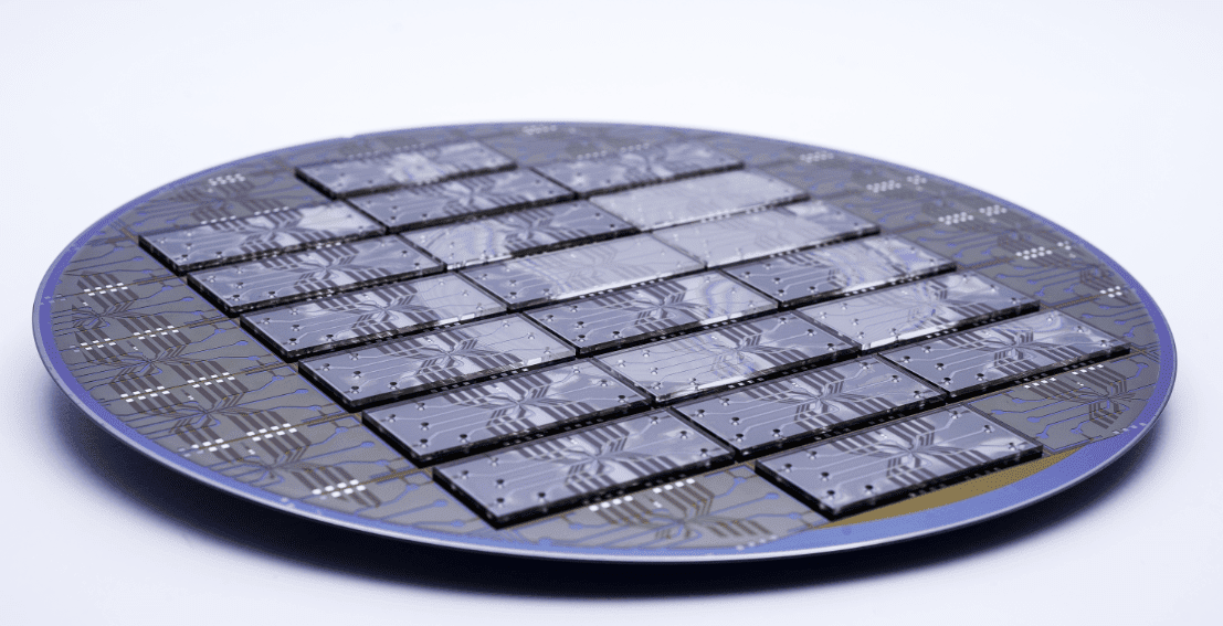
Imec, a world-leading nanoelectronics research center and JSR, a leading materials company, announce that they have successfully used JSR’s innovative PA (Photo-patternable Adhesive) material for wafer-scale processing of lab-on-chip devices. With PA as a key enabling material, imec has processed microfluidic cell-sorter devices, merging microheaters and sensors with wafer-scale polymer microfluidics. PA is a breakthrough material: a good microfluidic channel material and adhesive at the same time, suitable for wafer-scale processes and mass production.
Lab-on-chip technology will drive a revolution in medical technology in the years to come. It will enable powerful point-of-care diagnosis and treatment through on-chip molecular synthesis, separation, sensing, and detection. Key will be the ability to integrate microfluidics with heterogeneous components such as electronics, sensors, microheaters, and photonics in a cost-effective manner. To merge these elements successfully, new bonding and surface treatment materials are needed.
“PA solves a number of issues that we have with other materials, such as the widely-used PDMS (polydimethylsiloxane, a silicon-based organic polymer)”, says Liesbet Lagae, imec R&D manager of life science technologies. It has all the characteristics we are looking for in a photopatternable material to create microfluidic channels on silicon wafers, including a good channel definition and biocompatibility. But at the same time, it is an adhesive that allows direct thermal bonding with the cover glass. And unlike PDMS, it allows for wafer-scale processing, which is a prerequisite for industrial mass production.”
Imec used PA to process the next generation of its cell sorter lab-on-chip. Integrating on-chip imaging, in-flow cell tomography to identify cells, and bubble jet-flow technology to guide and sort individual cells, the prototype lab-on-chip can process up to 2,000 cells per second. One application envisaged for these ultrafast cell-sorters is the detection of circulating tumor cells in human blood.

Go deeper with Bing News on:
Mass production of lab-on-chip
- Chip Industry Week In Review
U.S. workforce hubs; Samsung's V-NAND chip; TSMC's A16 process and SoW; NVIDIA's AI acquisitions; IBM to acquire HashiCorp; China/Japan AI EV partnerships; MIT's secure digital IMC chip; a foundry ...
- TSMC unveils surprise A16 node, scheduled for mass production in 2026
The node will likely not make use of high-NA EUV lithography, the foundry says.
- New research demonstrates potential of thin-film electronics for flexible chip design
The mass production of conventional silicon chips relies on a successful business model with large "semiconductor fabrication plants" or "foundries." New research by KU Leuven and imec shows that this ...
- SK Hynix to invest $3.86 billion in DRAM chip production base in South Korea
The Nvidia supplier plans to start construction at the chip factory, called M15X, at the end of April with an aim to complete it by November 2025 for mass production. Including a planned gradual ...
- Feasibility of thin-film electronics for flexible chip design
(Nanowerk News) The mass production of conventional silicon chips relies ... after which they tested it in their lab, with success. The same chip was produced in two versions, based on two separate ...
Go deeper with Google Headlines on:
Mass production of lab-on-chip
[google_news title=”” keyword=”Mass production of lab-on-chip” num_posts=”5″ blurb_length=”0″ show_thumb=”left”]
Go deeper with Bing News on:
Lab on a chip
- Supreme Court decisions looming on abortion, guns, presidential immunity
The Supreme Court’s decisions this term will advance federal law on the powers of the presidency and the administrative state, and give the high court a chance to clarify major rulings in recent years ...
- China Shows Off Monkey With Brain Chip Allowing It to Control Robotic Arm
A Chinese company has announced that they have successfully developed a brain chip and implanted it into a monkey who can now remotely control a robot arm with the device, state-run news media outfit ...
- MIT Engineers Unveil Chip Boosting Smartphone AI and Security, Balancing Efficiency with Data Protection
MIT engineers developed a chip to protect personal data and enhance AI applications' efficiency in health-monitoring apps.
- Google Thinks It Can Cash In on Generative AI. Microsoft Already Has
While both Alphabet and Microsoft boasted strong quarterly earnings, only one tech giant showed that its generative AI bet is starting to pay off.
- New research demonstrates potential of thin-film electronics for flexible chip design
The mass production of conventional silicon chips relies on a successful business model with large "semiconductor fabrication plants" or "foundries." New research by KU Leuven and imec shows that this ...
Go deeper with Google Headlines on:
Lab on a chip
[google_news title=”” keyword=”lab on a chip” num_posts=”5″ blurb_length=”0″ show_thumb=”left”]