via University of Michigan
Researchers at North Carolina State University have developed a new technique for creating high-quality semiconductor thin films at the atomic scale – meaning the films are only one atom thick.
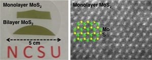
The technique can be used to create these thin films on a large scale, sufficient to coat wafers that are two inches wide, or larger.
“This could be used to scale current semiconductor technologies down to the atomic scale – lasers, light-emitting diodes (LEDs), computer chips, anything,” says Dr. Linyou Cao, an assistant professor of materials science and engineering at NC State and senior author of a paper on the work. “People have been talking about this concept for a long time, but it wasn’t possible. With this discovery, I think it’s possible.”
The researchers worked with molybdenum sulfide (MoS2), an inexpensive semiconductor material with electronic and optical properties similar to materials already used in the semiconductor industry. However, MoS2 is different from other semiconductor materials because it can be “grown” in layers only one atom thick without compromising its properties.
In the new technique, researchers place sulfur and molybdenum chloride powders in a furnace and gradually raise the temperature to 850 degrees Celsius, which vaporizes the powder. The two substances react at high temperatures to form MoS2. While still under high temperatures, the vapor is then deposited in a thin layer onto the substrate.
“The key to our success is the development of a new growth mechanism, a self-limiting growth,” Cao says. The researchers can precisely control the thickness of the MoS2 layer by controlling the partial pressure and vapor pressure in the furnace. Partial pressure is the tendency of atoms or molecules suspended in the air to condense into a solid and settle onto the substrate. Vapor pressure is the tendency of solid atoms or molecules on the substrate to vaporize and rise into the air.
To create a single layer of MoS2 on the substrate, the partial pressure must be higher than the vapor pressure. The higher the partial pressure, the more layers of MoS2 will settle to the bottom. If the partial pressure is higher than the vapor pressure of a single layer of atoms on the substrate, but not higher than the vapor pressure of two layers, the balance between the partial pressure and the vapor pressure can ensure that thin-film growth automatically stops once the monolayer is formed. Cao calls this “self-limiting” growth.
Partial pressure is controlled by adjusting the amount of molybdenum chloride in the furnace – the more molybdenum is in the furnace, the higher the partial pressure.
“Using this technique, we can create wafer-scale MoS2 monolayer thin films, one atom thick, every time,” Cao says. “We can also produce layers that are two, three or four atoms thick.”
Cao’s team is now trying to find ways to create similar thin films in which each atomic layer is made of a different material. Cao is also working to create field-effect transistors and LEDs using the technique. Cao has filed a patent on the new technique.
The Latest Bing News on:
Semiconductor technologies
- Chinese nationals accused of conspiring to export semiconductor technology from Santa Rosa firmon April 26, 2024 at 12:16 pm
Federal officials this week announced the unsealing of a December 2020 indictment that charged two Chinese nationals with illegally conspiring to export advanced semiconductor technology to a ...
- Taiwan Semiconductor's Options: A Look at What the Big Money is Thinkingon April 26, 2024 at 9:00 am
Maintaining their stance, an analyst from Barclays continues to hold a Overweight rating for Taiwan Semiconductor, targeting a price of $150. Maintaining their stance, an analyst from Barclays ...
- TSMC unveils A16, its 1.6nm chip process technology for 2026on April 26, 2024 at 5:24 am
Taiwanese semiconductor foundry TSMC has announced its 1.6nm chip process technology called A16. It enters production in 2026.
- On Semiconductor (NASDAQ:ON) Earnings Preview: Here’s What to Expect in Q1on April 26, 2024 at 4:08 am
On Semiconductor (NASDAQ:ON), also known as Onsemi, is slated to release its results for the first quarter of Fiscal 2024 before the market opens ...
- Japan to expand export curbs on chips, quantum technology - reporton April 26, 2024 at 3:54 am
Japan intends to expand restrictions on exports of four technologies related to semiconductors or quantum computing, Bloomberg News reported. The latest move, aimed at controlling the supply of ...
- Could Investing $15,000 in Axcelis Technologies Make You a Millionaire?on April 26, 2024 at 3:00 am
This company's equipment is quietly behind some of the world's biggest technological leaps -- and it's just getting started.
- Chinese National Arrested In U.S. For Alleged Role In Scheme To Illegally Export Semiconductor-Related Machineryon April 26, 2024 at 1:04 am
The export restrictions at issue in this case were put in place to prevent the illicit procurement of commodities and technologies for unauthorized military ...
- ASM Pacific Technology: Hold Rating Justified Amid Market Challenges and Growth Potentialon April 26, 2024 at 12:46 am
Analyst Jim Hin Kwong Au from DBS maintained a Hold rating on ASM Pacific Technology (ASMVF – Research Report) and keeping the price ...
- 3 Semiconductor Stocks That Could Be Multibaggers in the Making: April Editionon April 25, 2024 at 3:00 am
Stock Market News, Stock Advice & Trading Tips Semiconductors remain a red hot field of technology. Market analyst Charlie ...
- Biden to tout $6 billion deal with semiconductor manufacturer Micron during Syracuse tripon April 25, 2024 at 2:00 am
The Biden administration announced Thursday that it reached a preliminary agreement with Idaho-based semiconductor manufacturer Micron, the latest in a series of investments through the bipartisan ...
The Latest Google Headlines on:
Semiconductor technologies
[google_news title=”” keyword=”semiconductor technologies” num_posts=”10″ blurb_length=”0″ show_thumb=”left”]
The Latest Bing News on:
Thin films
- A better amorphous p-channel thin-film transistoron April 26, 2024 at 3:50 am
Scientist in Korea are making fast p-channel amorphous thin-film transistors. "Research progress on p-type amorphous semiconductors has been notably ...
- VideoFest Lives Again Alongside Denton’s Thin Line Feston April 24, 2024 at 2:11 pm
Bart Weiss, VideoFest’s founder, has partnered with Thin Line Fest to host two screenings that keep the independent spirit of VideoFest alive.
- Ultra-thin, flexible solar cells demonstrate their promise in a commercial quadcopter droneon April 24, 2024 at 9:27 am
Whether on Earth or in space, autonomous energy is critical in order to keep power systems running independently for extended periods of time, particularly in remote or unpredictable environments.
- New research demonstrates potential of thin-film electronics for flexible chip designon April 24, 2024 at 8:00 am
The mass production of conventional silicon chips relies on a successful business model with large "semiconductor fabrication plants" or "foundries." New research by KU Leuven and imec shows that this ...
- Feasibility of thin-film electronics for flexible chip designon April 23, 2024 at 5:00 pm
New research by KU Leuven and imec shows that this ‘foundry’ model can also be applied to the field of flexible, thin film electronics. Adopting this approach would give innovation in the field a huge ...
- Opening up the potential of thin-film electronics for flexible chip designon April 23, 2024 at 5:00 pm
The mass production of conventional silicon chips relies on a successful business model with large 'semiconductor fabrication plants' or 'foundries'. New research by shows that this 'foundry' model ...
- What to expect at Thin Line this week: Dallas VideoFest collab, films, local music and moreon April 23, 2024 at 12:26 pm
Thin Line Fest — which bills itself as the longest-running documentary film festival in Texas — will host film screenings at the Campus Theatre (and more) April 24-28. Most notably this year, this ...
- First Solar and ZSW collaborate on thin-film PV techon April 22, 2024 at 6:30 am
Leading solar company First Solar and research institute ZSW have announced a partnership to develop new technology for thin film solar PV. Based in Stuttgart, Germany, ZSW is a research institute ...
- New colorful plastic films for versatile sensors and electronic displayson April 19, 2024 at 11:40 am
Researchers have synthesized triarylborane (TAB) compounds that exhibit unusual optical responses upon binding to certain anions. They also synthesized thin polymer films that incorporate the TAB and ...
- Global Thin Film Battery Market Report 2023-2028: A $2.5 Billion Opportunity, Driven by Demand in Electronics, Medical Devices, and IoT Applicationson April 19, 2024 at 7:31 am
The "Thin Film Battery Market - Global Industry Size, Share, Trends, Opportunity, and Forecast, 2018-2028F" report has been added to ResearchAndMarkets.com's offering. This comprehensive research into ...
The Latest Google Headlines on:
Thin films
[google_news title=”” keyword=”thin films” num_posts=”10″ blurb_length=”0″ show_thumb=”left”]


