


Researchers at North Carolina State University have developed a new technique for creating high-quality semiconductor thin films at the atomic scale – meaning the films are only one atom thick.
The technique can be used to create these thin films on a large scale, sufficient to coat wafers that are two inches wide, or larger.
“This could be used to scale current semiconductor technologies down to the atomic scale – lasers, light-emitting diodes (LEDs), computer chips, anything,” says Dr. Linyou Cao, an assistant professor of materials science and engineering at NC State and senior author of a paper on the work. “People have been talking about this concept for a long time, but it wasn’t possible. With this discovery, I think it’s possible.”
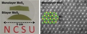
The researchers worked with molybdenum sulfide (MoS2), an inexpensive semiconductor material with electronic and optical properties similar to materials already used in the semiconductor industry. However, MoS2 is different from other semiconductor materials because it can be “grown” in layers only one atom thick without compromising its properties.
In the new technique, researchers place sulfur and molybdenum chloride powders in a furnace and gradually raise the temperature to 850 degrees Celsius, which vaporizes the powder. The two substances react at high temperatures to form MoS2. While still under high temperatures, the vapor is then deposited in a thin layer onto the substrate.
“The key to our success is the development of a new growth mechanism, a self-limiting growth,” Cao says. The researchers can precisely control the thickness of the MoS2 layer by controlling the partial pressure and vapor pressure in the furnace. Partial pressure is the tendency of atoms or molecules suspended in the air to condense into a solid and settle onto the substrate. Vapor pressure is the tendency of solid atoms or molecules on the substrate to vaporize and rise into the air.
To create a single layer of MoS2 on the substrate, the partial pressure must be higher than the vapor pressure. The higher the partial pressure, the more layers of MoS2 will settle to the bottom. If the partial pressure is higher than the vapor pressure of a single layer of atoms on the substrate, but not higher than the vapor pressure of two layers, the balance between the partial pressure and the vapor pressure can ensure that thin-film growth automatically stops once the monolayer is formed. Cao calls this “self-limiting” growth.
Partial pressure is controlled by adjusting the amount of molybdenum chloride in the furnace – the more molybdenum is in the furnace, the higher the partial pressure.
“Using this technique, we can create wafer-scale MoS2 monolayer thin films, one atom thick, every time,” Cao says. “We can also produce layers that are two, three or four atoms thick.”

Cao’s team is now trying to find ways to create similar thin films in which each atomic layer is made of a different material. Cao is also working to create field-effect transistors and LEDs using the technique. Cao has filed a patent on the new technique.
The Latest Bing News on:
Semiconductor technologies
- Vietnam poised to bridge global semiconductor workforce gapon May 8, 2024 at 11:17 pm
Vietnam has the potential to meet the global semiconductor workforce need in short, medium and long terms, Minister of Information and Communications Nguyen Manh Hung told a recent seminar, ...
- Lam Research tapping India for semiconductor wafer fabrication equipment components, says senior executiveon May 8, 2024 at 10:54 pm
With a comprehensive approach, the Ministry of Electronics & IT is also focusing on building the downstream ecosystem, including a comprehensive ecosystem for domestic manufacturing of semiconductor ...
- Saudi Arabia’s $100 Billion AI and Semiconductor Fund Signals Willingness to Divest from China at US Requeston May 8, 2024 at 9:49 pm
With substantial financial backing from Saudi Arabia’s Public Investment Fund, totaling a staggering $100 billion, Alat is positioned as a key player in the rapidly evolving landscape of artificial ...
- Saudi Arabia's $100 billion AI and semi-chip fund says it will divest from China if the US askson May 8, 2024 at 9:34 am
A new state-backed Saudi Arabian fund centered on semiconductor and AI technology has guaranteed that it would divest from China if Washington requests it. "US is the number one market, US is the ...
- 1 Super Semiconductor Stock Down 42% You'll Wish You'd Bought on the Dipon May 8, 2024 at 2:29 am
Axcelis Technologies is one of the cheapest stocks in the chip sector, and it's packed with long-term potential.
- Power Integrations To Acquire Assets Of Odyssey Semiconductor For Undisclosed Termson May 7, 2024 at 7:27 am
Power Integrations, Inc. (POWI) announced Tuesday an agreement to acquire the assets of Odyssey Semiconductor Technologies, a ...
- Biden's $285M boost for semiconductor innovation with cutting-edge techon May 7, 2024 at 6:04 am
President Joe Biden's administration has introduced a groundbreaking initiative aimed at bolstering American semiconductor manufacturing. At its heart is digital twin technology. Digital twins create ...
- Microchip to shut down semiconductor factories for two weeks amid inventory correctionon May 6, 2024 at 5:37 pm
Microchip Technology will shut down its Colorado Springs semiconductor factory for two weeks in June. Microchip Technology Inc. will move forward with a two-week shutdown in June at its three U.S.
- Arizona is poised for further momentum after TSMC, Intel and other semiconductor victorieson May 6, 2024 at 6:00 am
"There is critical mass — that’s the opportunity we have now in Arizona,” said Brian Harrison, president of TSMC Arizona.
- Bridging The Semiconductor Talent Gap With AI Copilots: A Strategic Dilemmaon May 6, 2024 at 5:30 am
The semiconductor industry is at a critical juncture, facing a significant talent gap that threatens to impede its growth and innovation.
The Latest Google Headlines on:
Semiconductor technologies
[google_news title=”” keyword=”semiconductor technologies” num_posts=”10″ blurb_length=”0″ show_thumb=”left”]
The Latest Bing News on:
Thin films
- Researchers identify cause of electron-hole separation in thin-film solar cells to increase solar cell efficiencyon May 8, 2024 at 6:38 am
A team of researchers have collaborated to characterize electron-hole separation in the light-absorbing layer of kesterite thin-film solar cells. This study is expected to improve the efficiency of ...
- Apple launches new films as it reveals its thinnest product ever: The 13-inch iPad Proon May 7, 2024 at 4:48 pm
Apple has revealed its thinnest product ever: the powerful new 13-inch iPad Pro. To accompany the launch, Apple has launched two films 'Crush' created in-house by Apple and 'iPad Vs. Nano: The ...
- Film Review: JEANNE DU BARRY (2023): Johnny Depp Falters in a Good-Looking but Disappointing Historical Dramaon May 5, 2024 at 6:31 pm
Jeanne du Barry (2023) Film Review, a movie directed by Maïwenn, written by Marion Pin, Teddy Lussi-Modeste and Maïwenn and starring Johnny Depp, Maïwenn, Benjamin Lavernhe, Pierre Richard, Robert ...
- Midsummer ties up with thin film solar panel maker Kaishengon May 2, 2024 at 10:27 pm
Swedish solar energy company Midsummer has started a collaboration with the Chinese manufacturer of thin film solar panels Kaisheng New Energy Technology. Kaisheng will produce thin film solar roof ...
- AI Powers Next-Gen Plastic-Film Recyclingon May 2, 2024 at 2:24 pm
Hyperspectral imaging technology uses deep-learning artificial intelligence to sort flexible packaging and other films rapidly and efficiently.
- Midsummer, Kaisheng partner on thin-film solar productionon May 1, 2024 at 5:00 pm
China’s Kaisheng New Energy Technology has agreed to produce a new line of thin-film solar panels for rooftops under an original equipment manufacturer (OEM) agreement with Sweden’s Midsummer. The ...
- Halfway to Halloween: The 13 best horror films of the year (so far)on April 30, 2024 at 12:00 pm
So, in honor of Halfway to Halloween, here are our picks for the best horror movies to get a wide release so far this year.
- Midsummer to build 200MW CIGS thin-film solar cell facility in Flen, Swedenon April 30, 2024 at 3:06 am
Swedish solar manufacturer Midsummer has selected the municipality of Flen in central Sweden to build a 200MW thin-film solar cell facility.
- Thin Film Semiconductor Deposition Market Analysis, Key Segments, Share, Size, Growth Status, and Forecast to 2024 to 2032on April 28, 2024 at 3:35 pm
Report Ocean has recently unveiled its research findings on the “Thin Film Semiconductor Deposition Market” spanning from 2024 to 2032. This comprehensive report thoroughly analyzes the market ...
- A better amorphous p-channel thin-film transistoron April 26, 2024 at 6:13 am
Scientist in Korea are making fast p-channel amorphous thin-film transistors. "Research progress on p-type amorphous semiconductors has been notably ...
The Latest Google Headlines on:
Thin films
[google_news title=”” keyword=”thin films” num_posts=”10″ blurb_length=”0″ show_thumb=”left”]

