


Courtesy of the researchers
Light-based devices could be used as biomedical sensors or as flexible connectors for electronics.
Researchers at MIT and several other institutions have developed a method for making photonic devices — similar to electronic devices but based on light rather than electricity — that can bend and stretch without damage. The devices could find uses in cables to connect computing devices, or in diagnostic and monitoring systems that could be attached to the skin or implanted in the body, flexing easily with the natural tissue.
The findings, which involve the use of a specialized kind of glass called chalcogenide, are described in two papers by MIT Associate Professor Juejun Hu and more than a dozen others at MIT, the University of Central Florida, and universities in China and France. The paper is slated for publication soon in Light: Science and Applications.
Hu, who is the Merton C. Flemings Associate Professor of Materials Science and Engineering, says that many people are interested in the possibility of optical technologies that can stretch and bend, especially for applications such as skin-mounted monitoring devices that could directly sense optical signals. Such devices might, for example, simultaneously detect heart rate, blood oxygen levels, and even blood pressure.
Photonics devices process light beams directly, using systems of LEDs, lenses, and mirrors fabricated with the same kinds of processes used to manufacture electronic microchips. Using light beams rather than a flow of electrons can have advantages for many applications; if the original data is light-based, for example, optical processing avoids the need for a conversion process.
But most current photonics devices are fabricated from rigid materials on rigid substrates, Hu says, and thus have an “inherent mismatch” for applications that “should be soft like human skin.” But most soft materials, including most polymers, have a low refractive index, which leads to a poor ability to confine a light beam.
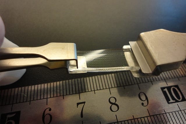
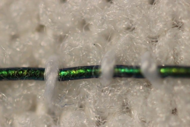
Instead of using such flexible materials, Hu and his team took a novel approach: They formed the stiff material — in this case a thin layer of a type of glass called chalcogenide — into a spring-like coil. Just as steel can be made to stretch and bend when formed into a spring, the architecture of this glass coil allows it to stretch and bend freely while maintaining its desirable optical properties.
“You end up with something as flexible as rubber, that can bend and stretch, and still has a high refractive index and is very transparent,” Hu says. Tests have shown that such spring-like configurations, made directly on a polymer substrate, can undergo thousands of stretching cycles with no detectable degradation in their optical performance. The team produced a variety of photonic components, interconnected by the flexible, spring-like waveguides, all in an epoxy resin matrix, which was made stiffer near the optical components and more flexible around the waveguides.
Other kinds of stretchable photonics have been made by embedding nanorods of a stiffer material in a polymer base, but those require extra manufacturing steps and are not compatible with existing photonic systems, Hu says.
Such flexible, stretchable photonic circuits could also be useful for applications where the devices need to conform to the uneven surfaces of some other material, such as in strain gauges. Optics technology is very sensitive to strain, according to Hu, and could detect deformations of less than one-hundredth of 1 percent.
This research is still in early stages; Hu’s team has demonstrated only single devices at a time thus far. “For it to be useful, we have to demonstrate all the components integrated on a single device,” he says. Work is ongoing to develop the technology to that point so that it could be commercially applied, which Hu says could take another two to three years.
In another paper published last week in Nature Photonics, Hu and his collaborators have also developed a new way of integrating layers of photonics, made of chalcogenide glass and two-dimensional materials such as graphene, with conventional semiconductor photonic circuitry. Existing methods for integrating such materials require them to be made on one surface and then peeled off and transferred to the semiconductor wafer, which adds significant complexity to the process. Instead, the new process allows the layers to be fabricated directly on the semiconductor surface, at room temperature, allowing for simplified fabrication and more precise alignment.
The process can also make use of the chalcogenide material as a “passivation layer,” to protect 2-D materials from degradation caused by ambient moisture, and as a way to control the optoelectronic characteristics of 2-D materials. The method is generic and could be extended to other emerging 2-D materials besides graphene, to expand and expedite their integration with photonic circuitry, Hu says.
Learn more: Researchers develop flexible, stretchable photonic devices
The Latest on: Photonic devices
[google_news title=”” keyword=”photonic devices” num_posts=”10″ blurb_length=”0″ show_thumb=”left”]- Utah delegation returns from trade mission to 'pivotal' Taiwan amid growing tensionson April 27, 2024 at 7:02 pm
Utah government, education and industry representatives traveled to Taiwan this month with the 47G association, developing partnerships as ...
- Light Brought 'To a Halt' in Quantum Breakthroughon April 26, 2024 at 10:16 am
The bizarre feat can be achieved in special, two-dimensional crystals by deforming them only slightly, a new study discovered.
- IPG Photonics (IPGP) to Post Q1 Earnings: What's in the Cards?on April 26, 2024 at 8:18 am
IPG Photonics' (IPGP) first-quarter 2024 results are likely to suffer from weakness in cutting and marking applications and sluggish demand in China market.
- Swave Photonics develops true holographic display for spatial computingon April 25, 2024 at 1:00 pm
Swave Photonics, a "true holographic display" company, announced the world’s first 3D holographic display technology for XR.
- Newark radio frequency systems manufacturer poised to get $700,000+ in state grantson April 25, 2024 at 6:03 am
AdvertisementPhase Sensitive Innovations (PSI) – a veteran-owned University of Delaware spinoff that specializes in radio-frequency components, devices and systems – will expand operations in Newark.
- Swave Photonics Developing World’s First True Holographic Display Technology To Power Reality-First Spatial Computingon April 25, 2024 at 2:00 am
April 25, 2024--(BUSINESS WIRE)--Swave Photonics, the true holographic display company ... The company is currently taking orders for HXR development kits for device manufacturers, which will reach ...
- Ultrasensitive photonic crystal detects single particles down to 50 nanometerson April 24, 2024 at 12:49 pm
Using an ultrasensitive photonic crystal, TU/e researchers were able to detect single particles down to 50 nanometers in diameter. The new research has just been published in the journal Optica.
- A shade closer to more efficient organic photovoltaicson April 24, 2024 at 10:00 am
Transparent solar cells will transform the look of infrastructure by enabling many more surfaces to become solar panels. Now, materials called non-fullerene acceptors that can intrinsically generate ...
- FRCC hosts mobile photonics lab through Thursdayon April 23, 2024 at 7:00 pm
A mobile lab set up at Front Range Community College through Thursday is providing visitors with an introduction to photonics with easy-to-understand, real-world applications.
- Study shines light on properties and promise of hexagonal boron nitride, used in electronic and photonics technologieson April 23, 2024 at 2:00 am
Single-photon emitters (SPEs) are akin to microscopic lightbulbs that emit only one photon (a quantum of light) at a time. These tiny structures hold immense importance for the development of quantum ...
via Google News and Bing News

