


These new materials work well up to 100 GHz, opening the door for the next generation of devices for advanced communications.
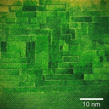
Researchers from the National Institute of Standards and Technology (NIST) have joined with an international team to engineer and measure a potentially important new class of nanostructured materials for microwave and advanced communication devices. Based on NIST’s measurements, the new materials—a family of multilayered crystalline sandwiches—might enable a whole new class of compact, high-performance, high-efficiency components for devices such as cellular phones.
“These materials are an excellent example of what the Materials Genome Initiative refers to as ‘materials-by-design’,” says NIST physicist James Booth, one of the lead researchers. “Materials science is getting better and better at engineering complex structures at an atomic scale to create materials with previously unheard-of properties.”
The new multilayer crystals are so-called “tunable dielectrics,” the heart of electronic devices that, for example, enable cell phones to tune to a precise frequency, picking a unique signal out of the welter of possible ones.
Tunable dielectrics that work well in the microwave range and beyond—modern communications applications typically use frequencies around a few gigahertz—have been hard to make, according to NIST materials scientist Nathan Orloff. “People have created tunable microwave dielectrics for decades, but they’ve always used up way too much power.” These new materials work well up to 100 GHz, opening the door for the next generation of devices for advanced communications.
Modern cellphone dielectrics use materials that suffer from misplaced or missing atoms called “defects” within their crystal structure, which interfere with the dielectric properties and lead to power loss. One major feature of the new materials, says Orloff, is that they self-correct, reducing the effect of defects in the part of the crystal where it counts. “We refer to this material as having ‘perfect faults’,” he says. “When it’s being grown, one portion accommodates defects without affecting the good parts of the crystal. It’s able to correct itself and create perfect dielectric bricks that result in the rare combination of high tuning and low loss.”
The new material has layers of strontium oxide, believed to be responsible for the self-correcting feature, separating a variable number of layers of strontium titanate. Strontium titanate on its own is normally a pretty stable dielectric—not really tunable at all—but another bit of nanostructure wizardry solves that. The sandwich layers are grown as a thin crystalline film on top of a substrate material with a mismatched crystal spacing that produces strain within the strontium titanate structure that makes it a less stable dielectric—but one that can be tuned. “It’s like putting a queen-sized sheet on a king-sized bed,” says Orloff. “The combination of strain with defect control leads to the unique electronic properties.”
One key discovery by the research team was that, in addition to adding strain to the crystal sandwich, adding additional layers of strontium titanate in between the strontium oxide layers increased the room-temperature “tunability” performance of the structure, providing a new mechanism to control the material response. The material they reported on recently in the journal Nature has six layers of strontium titanate between each strontium oxide layer.
The new sandwich material performs so well as a tunable dielectric, over such a broad range of frequencies, that the NIST team led by Booth had to develop a new measurement technique—an array of test structures fabricated on top of the test film—just to measure its electronic characteristics. “We were able to characterize the performance of these materials as a function of frequency running from 10 hertz all the way up to 125 gigahertz. That’s the equivalent of measuring wavelengths from kilometers down to microns all with the same experimental set-up,” says Orloff, adding, “This material has a much lower loss and a much higher tunability for a given applied field then any material that we have seen.”
Go deeper with Bing News on:
Tunable dielectrics
- Feed has no items.
Go deeper with Google Headlines on:
Tunable dielectrics
[google_news title=”” keyword=”Tunable dielectrics” num_posts=”5″ blurb_length=”0″ show_thumb=”left”]
Go deeper with Bing News on:
Nanostructured materials
- MC Physics well represented at EGLS-APS Spring 2024 Meeting
Marietta College was well represented at the Spring 2024 meeting of the Eastern Great Lakes Section (EGLS) of the American Physical Society (APS) in April at Kettering University in Flint, Michigan.
- Innovative scale-ups are transformers of Power+Utilities Australia
Now in the second year of its partnership, international incubator Startupbootcamp, will showcase the 15 new Australian companies with the potential to transform the energy transition journey in ...
- This alloy is kinky
Researchers have uncovered a remarkable metal alloy that won t crack at extreme temperatures due to kinking, or bending, of crystals in the alloy at the atomic level. Unlike most materials, the new ...
- Hong Kong wins a record-breaking number of awards in Geneva
The Hong Kong delegation has achieved a notable feat at the 49th International Exhibition of Inventions of Geneva, held from April 17 to 21. Comprising approximately 700 representatives from diverse ...
- Researchers develop ‘half-tandem’ perovskite solar cells with conversion efficiency of 27.63%
Khajeh Nasir Toosi University of Technology reserachers have developed ‘half-tandem’ solar cells with a power conversion efficiency of 27.63% ...
Go deeper with Google Headlines on:
Nanostructured materials
[google_news title=”” keyword=”nanostructured materials” num_posts=”5″ blurb_length=”0″ show_thumb=”left”]
