


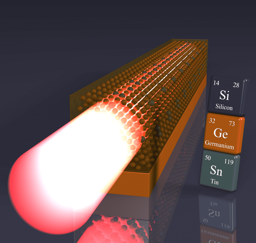
An international team of scientists constructs the first germanium-tin semiconductor laser for silicon chips
Scientists from Forschungszentrum Jülich and the Paul Scherrer Institute in Switzerland in cooperation with international partners have presented the first semiconductor consisting solely of elements of main group IV. As a consequence, the germanium-tin (GeSn) laser can be applied directly onto a silicon chip and thus creates a new basis for transmitting data on computer chips via light: this transfer is faster than is possible with copper wires and requires only a fraction of the energy. The results have been published in the journal Nature Photonics.
The transfer of data between multiple cores as well as between logic elements and memory cells is regarded as a bottleneck in the fast-developing computer technology. Data transmission via light could be the answer to the call for a faster and more energy efficient data flow on computer chips as well as between different board components. “Signal transmission via copper wires limits the development of larger and faster computers due to the thermal load and the limited bandwidth of copper wires. The clock signal alone synchronizing the circuits uses up to 30% of the energy – energy which can be saved through optical transmission,” explains Prof. Detlev Grützmacher, Director at Jülich’s Peter Grünberg Institute.
Some long-distance telecommunication networks and computing centres have been making use of optical connections for decades. They allow very high bandwidths even over long distances. Through optical fibres, signal propagation is almost lossless and possible across various wavelengths simultaneously: a speed advantage which increasingly benefits both micro- and nanoelectronics. “The integration of optical components is already well advanced in many areas. However, in spite of intensive research, a laser source that is compatible with the manufacturing of chips is not yet achievable,” according to the head of Semiconductor Nanoelectronics (PGI-9).
Suitable material for chip production
The basis of chip manufacturing is silicon, an element of main group IV of the periodic table. Typical semiconductor lasers for telecommunication systems, made of gallium arsenide for example, however, are costly and consist of elements from main groups III or V. This has profound consequences on the crystal properties. Such laser components cannot therefore be applied directly onto silicon. They have to be produced externally at great effort and subsequently glued to the silicon wafer. However, the lifetime of this kind of component is greatly reduced due to the fact that the thermal expansion coefficients of these elements are significantly different from that of silicon.
In contrast, semiconductors of main group IV – to which both silicon and germanium belong – can be integrated into the manufacturing process without any major difficulties. Neither element is very efficient as a light source, however. They are classed among the indirect semiconductors. In contrast to direct semiconductors, they emit mostly heat and only a little light when excited. That is why research groups all over the globe are intensively pursuing the objective of manipulating the material properties of germanium so that it would be able to amplify optical signals and thus make it a usable laser source.
Read more: New Laser for Computer Chips
The Latest on: Laser data transmission
[google_news title=”” keyword=”Laser data transmission” num_posts=”10″ blurb_length=”0″ show_thumb=”left”]
via Google News

The Latest on: MLaser data transmission
- Deep-space lasers smash data speed records over interplanetary distanceson May 6, 2024 at 12:07 am
NASA’s Psyche spacecraft, farther away than the Sun, has sent data through a laser over a record-breaking distance, and done so even faster than expected.
- Laser Transmission Explained: What It Means For Transmitting Data During Space Explorationon May 2, 2024 at 7:53 am
Some of the earliest spaceflights have been facilitated via radio communication with Earth, but laser transmission is the modern evolution of space comms.
- Earth receives laser signal from 140 million miles away: Here's what's happeningon May 2, 2024 at 2:54 am
NASA has recently received laser signals from deep space. These signals originated approximately 140 million miles away from the Earth. However, NASA has confirmed that the source is much closer to ...
- Earth picks up space laser transmission from 140 million miles away in major milestoneon April 30, 2024 at 4:29 am
The laser message was zapped Earthward by NASA's Deep Space Optical Communications transceiver mounted on the Psyche spacecraft.
- NASA uses laser link to beam data 140 million miles across space at 25 Mbpson April 29, 2024 at 12:31 pm
NASA has confirmed a significant milestone for its Psyche spacecraft's Deep Space Optical Communications (DSOC) experiment. This technology demonstration aims to test laser-based data links beyond ...
- Space laser transmission strikes Earth from 140 million miles away: NASAon April 29, 2024 at 8:11 am
Earth just received a laser transmission from a world (and perhaps universe) record-breaking 140 million miles away — which could have major implications for the future of space travel.
- Space laser transmission strikes Earth from 140 million miles away: NASAon April 29, 2024 at 8:11 am
Earth just received a laser transmission from a world- (and perhaps ... NASA managed to transmit actual data gathered from the spacecraft. “We downlinked about 10 minutes of duplicated ...
- NASA receives space laser message from 140 million miles awayon April 28, 2024 at 10:03 am
NASA's Psyche mission has shattered records, proving its capabilities in transmitting messages from deep space using lasers.
- NASA's laser communications demo sends data from over 140 million miles awayon April 25, 2024 at 11:22 pm
NASA’s Deep Space Optical Communications (DSOC), an experiment riding aboard the agency's Psyche spacecraft, recently sent a copy of engineering data from over 140 million miles (226 million ...
via Bing News

