The potential to conduct electrons five times faster than silicon
Researchers from Purdue and Harvard universities have created a new type of transistor made from a material that could replace silicon and have a 3-D structure instead of conventional flat computer chips.
The approach could enable engineers to build faster, more compact and efficient integrated circuits and lighter laptops that generate less heat than today’s. The transistors contain tiny nanowires made not of silicon, like conventional transistors, but from a material called indium-gallium-arsenide.
The device was created using a so-called “top-down” method, which is akin to industrial processes to precisely etch and position components in transistors. Because the approach is compatible with conventional manufacturing processes, it is promising for adoption by industry, said Peide “Peter” Ye, a professor of electrical and computer engineering at Purdue.
A new generation of silicon computer chips, due to debut in 2012, will contain transistors having a vertical structure instead of a conventional flat design. However, because silicon has a limited “electron mobility” — how fast electrons flow — other materials will likely be needed soon to continue advancing transistors with this 3-D approach, Ye said.
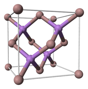
Indium-gallium-arsenide is among several promising semiconductors being studied to replace silicon. Such semiconductors are called III-V materials because they combine elements from the third and fifth groups of the periodic table.
“Industry and academia are racing to develop transistors from the III-V materials,” Ye said. “Here, we have made the world’s first 3-D gate-all-around transistor on much higher-mobility material than silicon, the indium-gallium-arsenide.”
Findings will be detailed in a paper to be presented during the International Electron Devices Meeting on Dec. 5-7 in Washington, D.C. The work is led by Purdue doctoral student Jiangjiang Gu; Harvard doctoral student Yiqun Liu; Roy Gordon, Harvard’s Thomas D. Cabot Professor of Chemistry; and Ye.
Transistors contain critical components called gates, which enable the devices to switch on and off and to direct the flow of electrical current. In today’s chips, the length of these gates is about 45 nanometers, or billionths of a meter. However, in 2012 industry will introduce silicon-based 3-D transistors having a gate length of 22 nanometers.
“Next year if you buy a computer it will have the 22-nanometer gate length and 3-D silicon transistors,” Ye said.
The 3-D design is critical because the 22-nanometer gate lengths will not work in a flat design.
“Once you shrink gate lengths down to 22 nanometers on silicon you have to do more complicated structure design,” Ye said. “The ideal gate is a necklike, gate-all-around structure so that the gate surrounds the transistor on all sides.”
The nanowires are coated with a “dielectric,” which acts as a gate. Engineers are working to develop transistors that use even smaller gate lengths, 14 nanometers, by 2015.
However, further size reductions beyond 14 nanometers and additional performance improvements are likely not possible using silicon, meaning new designs and materials will be needed to continue progress, Ye said.
“Nanowires made of III-V alloys will get us to the 10 nanometer range,” he said.
The new findings confirmed that the device made using a III-V material has the potential to conduct electrons five times faster than silicon.
Bookmark this page for “3D transistors” and check back regularly as these articles update on a very frequent basis. The view is set to “news”. Try clicking on “video” and “2” for more articles.


