


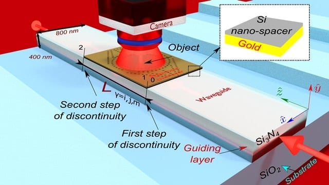
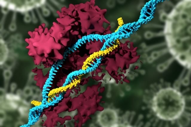
According to the recent study Invisibility Cloaking Scheme by Evanescent Distortion on Composite Plasmonic Waveguides with Si Nano-Spacer? published in Nature Scientific Reports?, the researchers conceived a new method that deflects and scatters light away from a “cloaking” chip surface so it is not detected.
An operational cloaking chip can be an extension of the basic technologies such as radar-absorbing dark paint used on stealth aircraft, local optical camouflage, surface cooling to minimize electromagnetic infrared emissions, or electromagnetic wave scattering.
“These results open the door to new integrated photonic devices, harnessing electromagnetic fields of light at nanoscale for a variety of applications from on-chip optical devices to all-optical processing,” says Dr. Alina Karabchevsky (pictured left), head of BGU’s Light-o?n-a-Chip Group and a member of BGU’s Unit of Electro-Optical Engineering and the Ilse Katz Institute for Nanoscale Science and Technology. “We showed that it is possible to bend the light around an object located on the cloak on an optical chip. The light does not interact with the object, thus resulting in the object’s invisibility.”
The next step is for researchers to overcome the significant challenge of developing a prototype.
Learn more: BGU Researchers Achieve Breakthrough in Camouflaging an Optical Chip Rendering it Invisible
The Latest on: Cloaking chip
[google_news title=”” keyword=”cloaking chip” num_posts=”10″ blurb_length=”0″ show_thumb=”left”]- These shocking aerial images show the threat of climate actionon May 1, 2024 at 11:00 am
Depicting everything from dried-up waterways to cities shrouded in smog, these aerial photographs show the devastation of the climate crisis.
- Bawumia must be truthful with the people of Eastern Region on his campaign tour, we're readily prepared to expose his lies – NDCon April 29, 2024 at 8:59 am
The Eastern Regional Communications Officer of the opposition National Democratic Congress NDC, Comrade Kojo Danquah, has urged Dr Mahamudu Bawumia, the flagbearer of the ruling New Patriotic Party ...
- The RSPB Big Garden Birdwatch 2024 results are in, and pigeons and tits are top of the pops - Gaby Soutaron April 27, 2024 at 9:55 pm
They are in decline, so let them eat chips. It’s not like our equally scavenge-y species ... half dinosaur. When he spreads his cloak-like wings, to warm up, everyone on the path takes photographs and ...
- FCC officially votes to reinstate net neutralityon April 25, 2024 at 10:30 am
The Federal Communications Commission made its official vote Thursday to reinstate net neutrality, passing an order titled Safeguarding and Securing the Open Internet. This restores, with some changes ...
- Transgender People: Every Vote Counts, and We Take Our Responsibility Seriouslyon April 25, 2024 at 4:40 am
They have instantly warmed up to me, said Raju.Kumbar said to take this further, transgender people need to be given reservation in political representation, jobs and education.
- Green Vodka Sauce and Lasagna Chips at a New Brooklyn Restauranton April 19, 2024 at 7:50 am
The 50-seat restaurant located at 299 Halsey Street, at Throop Avenue in Bed-Stuy, sticks to hues of greens and purples, with walls covered with old New York Philharmonic ephemera, and a ball-chain ...
- Bleeding Cool Presents Image Comics Full July 2024 Solicitson April 19, 2024 at 6:01 am
Founder of Bleeding Cool. The longest-serving digital news reporter in the world, since 1992. Author of The Flying Friar, Holed Up, The Avengefuls, Doctor Who: Room With A Deja Vu, The Many Murders Of ...
- From Colorado to transfer portal, is there a path of redemption for Cormani McClain?on April 18, 2024 at 9:21 am
McClain was tabbed as a future superstar as the nation's No. 14 overall prospect and No. 1 cornerback out of Lakeland (Fla.) High in 2023. He tumbled Tuesday in 247Sports' Transfer Portal rankings as ...
- Donald Trump not in court today for hush money trial after vow to ‘straighten NY out’on April 17, 2024 at 4:35 am
Trump stopped by Sanaa Convenient Store, a tiny bodega that sells chips, sodas and other snacks on Tuesday after ... Prosecutors say the payments to Cohen were falsely logged as legal fees to cloak ...
- First day of historic Trump trial ends without any jurors being pickedon April 15, 2024 at 3:30 pm
The historic hush-money trial of Donald Trump got underway Monday with the arduous process of selecting a jury to hear the case charging the former president with falsifying business records to stifle ...
via Google News and Bing News