


New optical technologies using “metasurfaces” capable of the ultra-efficient control of light are nearing commercialization, with potential applications including advanced solar cells, computers, telecommunications, sensors and microscopes.
The metasurfaces could make possible “planar photonics” devices and optical switches small enough to be integrated into computer chips for information processing and telecommunications, said Alexander Kildishev, associate research professor of electrical and computer engineering at Purdue University.
“I think we know enough at this point that we can realistically start to develop prototypes of devices for some applications,” he said.
The promise of metasurfaces is described in an article appearing Friday (March 15) in the journal Science. The article was co-authored by Kildishev; Alexandra Boltasseva, an assistant professor of electrical and computer engineering; and Vladimir M. Shalaev, scientific director of nanophotonics at Purdue’s Birck Nanotechnology Center and a distinguished professor of electrical and computer engineering.
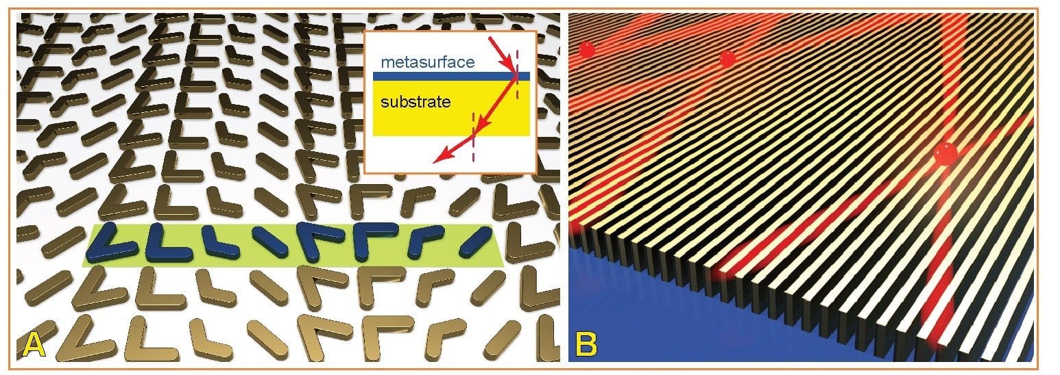
The metasurfaces are extremely thin films of “metamaterials,” assemblies that contain features, patterns or elements such as tiny antennas or alternating layers of oxides that enable an unprecedented control of light. Under development for about 15 years, the metamaterials owe their unusual potential to precision design on the scale of nanometers.
Optical nanophotonic circuits might harness clouds of electrons called “surface plasmons” to manipulate and control the routing of light in devices too tiny for conventional lasers.
The metasurfaces are typically created using electron-beam lithography or focused ion beam milling and may also be made of materials that are compatible with existing semiconductor manufacturing and industrial processes.
“That is one of the attractive features of metasurfaces,” Kildishev said. “If we use certain types of plasmonic material, they can be integrated into existing semiconductor processes, which makes them practical for commercialization.”
Plasmonic metamaterials are promising for various advances, including a possible “hyperlens” that could make optical microscopes 10 times more powerful; advanced chemical sensors; new types of light-harvesting systems for more efficient solar cells; computers and consumer electronics that use light instead of electronic signals to process information; and a cloak of invisibility.
The metasurfaces can be combined with thin sheets of carbon called graphene.
“If you apply voltage the optical properties of graphene change, and if you couple a graphene layer with a metasurface, these properties then change dramatically,” Kildishev said.
Metasurfaces could make it possible to use single photons – the tiny particles that make up light – for switching and routing in future computers. While using photons would dramatically speed up computers and telecommunications, conventional photonic devices cannot be miniaturized because the wavelength of light is too large to fit in tiny components needed for integrated circuits.
Nanostructured metamaterials, however, could make it possible to reduce the size of photons and the wavelength of light, allowing the creation of new types of nanophotonic devices, Shalaev said.
Some of the new materials may have applications involving near-infrared light, the range of the spectrum critical for telecommunications and fiberoptics. Other materials also might work for light in the spectrum’s visible range.
Unlike natural materials, metamaterials may possess an index of refraction less than one or less than zero. Refraction occurs as electromagnetic waves, including light, bend when passing from one material into another. It causes the bent-stick-in-water effect, which occurs when a stick placed in a glass of water appears crooked when viewed from the outside. Being able to create materials with an index of refraction that’s negative or between one and zero promises a range of potential breakthroughs in a new field called transformation optics.
The Latest Bing News on:
Metasurfaces
- This Could Kill The iPhone Notch, Bring Cheap FaceID To Android, And Medical Apps To Your Cameraon April 30, 2024 at 12:03 pm
Phone has this face unlock feature, but it really hasn’t propagated outside of the iPhone because that module is very expensive, very complicated, and ..." ...
- Gigahertz-rate switchable wavefront shaping by LNOI-empowered metasurfaceon April 15, 2024 at 5:00 pm
More information: Haozong Zhong et al, Gigahertz-rate-switchable wavefront shaping through integration of metasurfaces with photonic integrated circuit, Advanced Photonics (2024). DOI: 10.1117/1 ...
- Safeguarding the future of online security with AI and metasurfaceson April 15, 2024 at 1:18 pm
More information: Joohoon Kim et al, Dynamic Hyperspectral Holography Enabled by Inverse‐Designed Metasurfaces with Oblique Helicoidal Cholesterics, Advanced Materials (2024). DOI: 10.1002/adma.
- Propagating dimensions of light: Deforming versatile non-diffractive beams along the optical trajectoryon April 7, 2024 at 5:00 pm
The development of metasurfaces has brought new changes, using the precise arrangement of nanoscale antenna arrays to miniaturize optical devices and achieve multidimensional control of light ...
- Intelligent metasurfaces enable ultra-high performance passive radiative coolingon April 4, 2024 at 11:27 am
A new publication from Opto-Electronic Advances; DOI 10.29026/oea.2024.230194, discusses intelligent metasurfaces enable ultra-high performance passive radiative cooling. Daytime passive radiative ...
- Dielectric meta-atoms with liquid crystal alignment effect for electrically tunable metasurfaceon March 31, 2024 at 5:00 pm
Dielectric metasurfaces represent one of the cutting-edge research and application directions in the current optical field. They not only possess the advantage of low loss but also enable the ...
- Angle-dependent holograms made possible by metasurfaceson February 21, 2024 at 10:16 am
The team addressed this challenge by leveraging metasurfaces, artificial nanostructures capable of precisely manipulating the characteristics of light. These metasurfaces are incredibly thin and ...
- Hualiang Zhangon August 4, 2023 at 12:27 pm
Applied electromagnetics; Metasurfaces and metamaterials; High frequency circuits and systems; Flexible electronics Metasurface and metamaterials; antenna design; RF ...
- Elena Semouchkinaon April 6, 2021 at 12:27 am
Semouchkina is the author of the book “Dielectric Metamaterials and Metasurfaces in Transformation Optics and Photonics” published by ELSEVIER, Woodhead Publishing Series in Electronic and Optical ...
- Metamaterials and Metasurfaces: Engineered Structures Revolutionizing Light and Matter Interactionson August 18, 2020 at 1:09 pm
You can also manipulate the light with the help of two-dimensional (2D) structures – so-called metasurfaces (or flat optics or meta-optics). Metasurfaces are thin-films composed of individual elements ...
The Latest Google Headlines on:
Metasurfaces
[google_news title=”” keyword=”metasurfaces” num_posts=”10″ blurb_length=”0″ show_thumb=”left”] [/vc_column_text]The Latest Bing News on:
Metamaterials
- SkyWater and Lumotive Announce Qualification and Production Start for World’s First Commercially Available Optical Beamforming Chipon May 1, 2024 at 4:05 am
SkyWater Technology (NASDAQ: SKYT), the trusted technology realization partner, and Lumotive, a pioneer in optical semiconductor technology for 3D sensing, announced today that the companies have ...
- New “Metafluid” Liquid Can Be Programmed To Adapt To Different Situations It Encounterson April 27, 2024 at 6:32 am
Researchers say they believe this is an intriguing development in the fairly new field of metamaterials. Their “intelligent liquid” has a unique structure that allows it to alter its properties ...
- Dark matter: A new experiment aims to turn the ghostly substance into actual lighton April 26, 2024 at 9:55 am
A ghost is haunting our universe. This has been known in astronomy and cosmology for decades. Observations suggest that about 85% of all the matter in the universe is mysterious and invisible. These ...
- Programmable liquid hints at widespread applicationson April 26, 2024 at 7:38 am
A 'metafluid' formed from collapsible elastic shells suspended in oil exhibits very different properties at different pressures ...
- Metamaterials articles from across Nature Portfolioon April 4, 2024 at 5:00 pm
Metamaterials are engineered structures designed to interact with electromagnetic radiation in a desired fashion. They usually comprise an array of structures smaller than the wavelength of interest.
- Team demonstrates an ultra-broadband tunable terahertz absorber of graphene and hierarchical plasmonic metamaterialson April 1, 2024 at 12:56 pm
Compared to static passive physical systems, tunable metamaterials can dynamically manipulate electromagnetic waves, improving multidimensional control of the optical response. There are two ...
- Metamaterials and Metasurfaces: Engineered Structures Revolutionizing Light and Matter Interactionson August 18, 2020 at 1:09 pm
What are metamaterials and what can they do? The prefix meta (a Greek word meaning ‘beyond’) indicates that the characteristics of the material are beyond what we see in nature. Metamaterials are a ...
- MECH_ENG 495: Metamaterialson August 12, 2020 at 7:46 pm
Metamaterials that mimic the order in matters have opened an exciting gateway to reach unprecedented physical properties and functionality unattainable from naturally existing materials. The "atoms" ...
- Emerging Theories and Technologies in Metamaterialson February 7, 2018 at 2:47 pm
Bringing together viewpoints of leading scientists and engineers, this new series provides systematic coverage of new and emerging topics in metamaterials. Elements cover the theory, characterisation, ...
- MECH.6150 Micromechanics of Composites and Metamaterialson November 18, 2016 at 1:03 pm
Overall behavior of composite materials and metamaterials. The fundamentals of homogenization for elastic composites, variational principles and energy-based bounds, and dynamic homogenization ...
The Latest Google Headlines on:
Metamaterials
[google_news title=”” keyword=”metamaterials” num_posts=”10″ blurb_length=”0″ show_thumb=”left”]

