


Tremendous potential of this material for future low-power and high-performance integrated circuits
UC Santa Barbara researchers demonstrate first n-type field effect transistors on monolayer tungsten diselenide with record performance
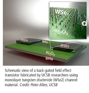
Researchers at UC Santa Barbara, in collaboration with University of Notre Dame, have recently demonstrated the highest reported drive current on a transistor made of a monolayer of tungsten diselenide (WSe2), a 2-dimensional atomic crystal categorized as a transition metal dichalcogenide (TMD). The discovery is also the first demonstration of an “n-type” WSe2 field-effect-transistor (FET), showing the tremendous potential of this material for future low-power and high-performance integrated circuits.
Monolayer WSe2 is similar to graphene in that it has a hexagonal atomic structure and derives from its layered bulk form in which adjacent layers are held together by relatively weak Van der Waals forces. However, WSe2 has a key advantage over graphene.
“In addition to its atomically smooth surfaces, it has a considerable band gap of 1.6 eV,” explained Kaustav Banerjee, professor of electrical and computer engineering and Director of the Nanoelectronics Research Lab at UCSB. Banerjee’s research team also includes UCSB researchers Wei Liu, Jiahao Kang, Deblina Sarkar, Yasin Khatami and Professor Debdeep Jena of Notre Dame. Their study was published in the May 2013 issue of Nano Letters.
“There is growing worldwide interest in these 2D crystals due to the many possibilities they hold for the next generation of integrated electronics, optoelectronics and sensors,” commented Professor Pulickel Ajayan, the Anderson Professor of Engineering at Rice University and a world renowned authority on nanomaterials. “This result is very impressive and an outcome of the detailed understanding of the physical nature of the contacts to these 2D crystals that the Santa Barbara group has developed.”
“Understanding the nature of the metal-TMD interfaces was key to our successful transistor design and demonstration,” explained Banerjee. Banerjee’s group pioneered a methodology using ab-initio Density Functional Theory (DFT) that established the key criteria needed to evaluate such interfaces leading to the best possible contacts to the monolayer TMDs.
The DFT technique was pioneered by UCSB professor emeritus of physics Dr. Walter Kohn, for which he was awarded the Nobel Prize in Chemistry in 1998. “At a recent meeting with Professor Kohn, we discussed how this relatively new class of semiconductors is benefitting from one of his landmark contributions,” said Banerjee.
The Latest Bing News on:
Integrated circuits
- Power Management Integrated Circuit Market is Poised to Reach USD 54.69 Billion By 2032: Astute Analyticaon April 30, 2024 at 1:30 am
New Delhi, April 30, 2024 (GLOBE NEWSWIRE) -- The global power management integrated circuit market is expected to experience significant growth, with a projected market valuation of US$ 54.69 billion ...
- Oppstar partners with Samsung to produce industrial integrated circuitson April 29, 2024 at 10:07 am
Integrated circuit (IC) design service provider Oppstar Bhd is collaborating with South Korea’s tech giant Samsung Electronics Co Ltd for the production of industrial ICs manufactured using Samsung’s ...
- Oppstar partners with Samsung Electronics for industrial integrated circuit productionon April 29, 2024 at 3:30 am
Oppstar Bhd, via wholly-owned subsidiary Oppstar Technology Sdn Bhd and Samsung Electronics Co Ltd, have proposed to cooperate and collaborate for the production of industrial integrated circuits (IC) ...
- Flexible Printed Circuit Boards Market Latest Trends, Size, Key Players, Revenue, Growth, and Forecast to 2024 to 2032on April 28, 2024 at 3:13 pm
Report Ocean has recently unveiled its research findings on the “Flexible Printed Circuit Boards Market” spanning from 2024 to 2032. This comprehensive report thoroughly analyzes the market dynamics, ...
- Power Management Integrated Circuits (PMICs) Market Size, Share, Key Players, Revenue, Demand, and Forecast 2024 to 2032on April 28, 2024 at 3:10 pm
Report Ocean has recently unveiled its research findings on the “Power Management Integrated Circuits (PMICs) Market” spanning from 2024 to 2032. This comprehensive report thoroughly analyzes the ...
- Malaysia to have region's largest integrated circuit design parkon April 26, 2024 at 2:43 am
This week, the Malaysian government said it plans to build Southeast Asia's largest integrated circuit design park ...
- Transphorm and Weltrend Semiconductor Release New Integrated GaN System-in-Packageson April 24, 2024 at 5:42 am
Weltrend's SuperGaN SiP family is optimized for use in high-performance, low-profile USB-C power adapters for mobile/IoT devices such as smartphones, tablets, laptops, headphones, drones, speakers, ...
- Malaysia plans Southeast Asia's largest integrated circuit design parkon April 21, 2024 at 8:44 pm
Malaysia plans to build Southeast Asia's largest integrated circuit design park and will offer incentives including tax breaks, subsidies and visa exemption fees to attract global tech companies and ...
- IDTechEx Release New Global Silicon Photonics and Photonic Integrated Circuits Market Reporton April 19, 2024 at 6:38 am
IDTechEx Research, a trusted provider of independent market intelligence, announces the availability of a new report, "Silicon Photonics and Photonic Integrated Circuits 2024-2034: Market, ...
- Keysight introduces next-generation radio frequency circuit simulatoron April 18, 2024 at 11:43 am
Keysight Technologies has introduced RFPro Circuit, a next-generation radio frequency (RF) simulation tool.
The Latest Google Headlines on:
Integrated circuits
[google_news title=”” keyword=”integrated circuits” num_posts=”10″ blurb_length=”0″ show_thumb=”left”]
The Latest Bing News on:
Low-power and high-performance integrated circuits
- A new framework to improve high computing performanceon April 30, 2024 at 2:03 pm
From a luxury to a day-to-day necessity, computing isn't quite what it used to be. As applications like machine learning and 5G mobile networks become the norm, the need for high computing performance ...
- HMI Introduces a Single-Channel 80 mO High-Side Switch Ideal for Automotive Applicationson April 30, 2024 at 3:41 am
HMI, a leading provider of advanced analog and power management technologies, today announced the launch of its HL8518, a single-chip 80 mO high-side switch ideal for automotive applications needing ...
- HMI Introduces a Single-Channel 80 mΩ High-Side Switch Ideal for Automotive Applicationson April 30, 2024 at 2:59 am
HMI, a leading provider of advanced analog and power management technologies, today announced the launch of its HL8518, a single-chip 80 mΩ high-side switch ideal for automotive applications needing ...
- STMicroelectronics reveals high-performance wireless microcontrollers for incoming cyber-protection regulationson April 29, 2024 at 12:31 am
Highly integrated chips support multiple wireless technologies and latest security standards, perfectly addressing requirements for smart industrial, medical, and consumer devices.
- Digital Power Management Multichannel IC Market CAGR of 16.3%, Latest Trends, Segmentation Analysis, Share, Size, and Forecast 2024 to 2032on April 28, 2024 at 11:07 pm
Power management multichannel integrated circuits (PMICs ... Growth in demand for low power consumption and high-performance devices is expected to provide an opportunity to the market growth.
- The real reason so many laptops have moved to soldered RAMon April 27, 2024 at 8:00 am
There are some glaring downsides to using soldered RAM. Laptop manufacturers can get away with them, because hey, for many users it just doesn’t matter. However, for those who care, the laptop market ...
- Researcher develop high-performance amorphous p-type oxide semiconductoron April 26, 2024 at 6:56 am
Researchers have collaborated on the development of a tellurium-selenium composite oxide semiconductor material. Their efforts led to the successful creation of a high-performance and highly stable ...
- Professor resolves two decades of oxide semiconductor challengeson April 25, 2024 at 5:00 pm
Successful development of high-performance amorphous P-type oxide semiconductor using tellurium-selenium composite oxide.
- Breakthrough in high-performance amorphous semiconductor developmenton April 25, 2024 at 5:00 pm
This setback has hindered the development of n-p-type complementary metal oxide semiconductors (CMOS), which serve as the cornerstone of electronic devices and integrated circuits. Achieving ...
- Transphorm and Weltrend Semiconductor Release New Integrated GaN System-in-Packageson April 24, 2024 at 5:42 am
Weltrend's SuperGaN SiP family is optimized for use in high-performance, low-profile USB-C power adapters for mobile/IoT devices such as smartphones, tablets, laptops, headphones, drones, speakers, ...
The Latest Google Headlines on:
Low-power and high-performance integrated circuits
[google_news title=”” keyword=”low-power and high-performance integrated circuits” num_posts=”10″ blurb_length=”0″ show_thumb=”left”]

