


In the semiconductor business, it is called the “red brick wall” — the limit of the industry’s ability to shrink transistors beyond a certain size.
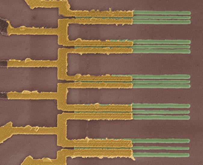
On Thursday, however, IBM scientists reported that they now believe they see a path around the wall. Writing in the journal Science, a team at the company’s Thomas J. Watson Research Center said it has found a new way to make transistors from parallel rows of carbon nanotubes.
The advance is based on a new way to connect ultrathin metal wires to the nanotubes that will make it possible to continue shrinking the width of the wires without increasing electrical resistance.
One of the principal challenges facing chip makers is that resistance and heat increase as wires become smaller, and that limits the speed of chips, which contain transistors.
The advance would make it possible, probably sometime after the beginning of the next decade, to shrink the contact point between the two materials to just 40 atoms in width, the researchers said. Three years later, the number will shrink to just 28 atoms, they predicted.
The ability to reduce electrical resistance will not only make it possible to extend the process of shrinking transistors beyond long-held beliefs about physical limits. It may also be the key to once again increasing the speed of computer processors, which has been stalled for the last decade.
The report represents a big advance for an exotic semiconductor material that has long held great promise but has also proved maddeningly difficult for scientists to work with. Single-wall carbon nanotubes are strawlike structures that are a composed of a one-atom thick matrix of carbon atoms rolled into an infinitesimally small tube.
The challenge of carbon nanotubes in their typical state is that they form what scientists call a giant “hairball” of interwoven molecules.
However, researchers have found ways to align them closely and in regularly spaced rows and deposit them on silicon wafers with great precision. They then serve the crucial role of a semiconductor, allowing electrical current to be switched on and off in a computer circuit.
Until now, however, they have been just one of a range of new materials that have been seen as candidates to replace silicon, which has for more than half a century been the material of choice for chip makers.
“Of all the possible materials, this one is at the top of the list by a long shot,” said Dario Gil, vice president for science and technology at IBM Research.
Read more: IBM Scientists Find New Way to Shrink Transistors

The Latest on: Transistors
[google_news title=”” keyword=”Transistors” num_posts=”10″ blurb_length=”0″ show_thumb=”left”]
via Google News
The Latest on: Transistors
- Smartkem To Exhibit and Present at Display Week 2024on May 1, 2024 at 1:00 am
MANCHESTER, England, May 1, 2024 /PRNewswire/ -- Smartkem (OTCQB: SMTK), the developer of a new class of semiconductor polymer transistors with the potential to power the next generation of displays, ...
- “Magnetisation switching” can replace transistors, cutting energy demand from computing by an order of magnitudeon May 1, 2024 at 12:07 am
Globally, energy demand from computing is growing so fast the search is on to find fundamental ways to make it more efficient. “Magnetisation switching” has long been seen as a more efficient way than ...
- Organic electrochemical transistors: Scientists solve chemical mystery at the interface of biology and technologyon April 30, 2024 at 11:22 am
Researchers who want to bridge the divide between biology and technology spend a lot of time thinking about translating between the two different "languages" of those realms.
- Samsung to Introduce 3rd Generation Gate-All-Around 2nm Transistors in 2025on April 30, 2024 at 10:00 am
The company is already the industry leader when it comes to gate-all-around transistors, but so far it's yet to really make a dent in TSMC's market share.
- N-Type Diamond Transistors: New Semiconductor Standardson April 30, 2024 at 2:33 am
Diamond transistors open new avenues for advanced electronic systems, offering unparalleled durability and efficiency.
- Insulated-Gate Bipolar Transistors (IGBTs) Market Size, Share, Key Players, Revenue, Demand, and Forecast to 2024 to 2032on April 28, 2024 at 3:31 pm
Report Ocean has recently unveiled its research findings on the “Insulated-Gate Bipolar Transistors (IGBTs) Market” spanning from 2024 to 2032. This comprehensive report thoroughly analyzes the market ...
- TSMC System on Wafer for Over 3.5 Times the Compute by 2027on April 27, 2024 at 5:00 pm
At the TSMC 2024 North America Technology Symposium, they debuted the TSMC A16™ technology, featuring leading nanosheet transistors with innovative backside power rail solution for production in 2026, ...
- TSMC races for chip supremacy with new A16 process for AI-ready futureon April 25, 2024 at 2:37 am
With its focus on nanosheet transistors and innovative backside power delivery, A16 paves the way for the production of 1.6nm chips by 2026.
- Exynos 2500 could be more efficient than Snapdragon 8 Gen 4 thanks to use of GAA transistorson April 18, 2024 at 7:44 pm
In 2023, all Galaxy S23 models were equipped with the Snapdragon 8 Gen 2 for Galaxy chipset. Samsung did not mass-produce the Exynos 2300. This year, with the Exynos 2400 capable of driving a flagship ...
- Machine at Intel's Hillsboro campus can produce chips so advanced, they don't yet existon April 18, 2024 at 6:49 pm
At the Gordon Moore campus, Intel engineers do the work to push Moore's Law — the idea that the number of transistors on a single chip will double every two years.
via Bing News
