


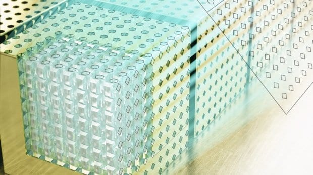
Scientists at the University of Twente’s MESA+ research institute have developed a new manufacturing method to create three-dimensional nanostructures. This revolutionary method enables large-scale production of photonic crystals that can capture light. The discovery also makes it possible to produce chips with additional functions for mobile devices, computers and other applications. The researchers’ findings was published today in Nanotechnology, the leading journal of the British Institute of Physics.
The conventional method for manufacturing 3D nanostructures consists of stacking layers on a silicon chip. The first step is to write (or define) a pattern in the photoresist, using a mask and UV light. The etching or deposition of material in the layer then provides the desired shape. Dozens of layers are stacked to produce the chips themselves. This is a laborious process with limitations. There are restrictions on the number of layers that can be stacked, since layers that are relatively far apart can become randomly displaced with respect to one another, interfering with the chip’s functionality.
SINGLE PROCESS
The new method makes it possible to define a 3D nanostructure on a chip in a single process. Researchers from the University of Twente’s MESA+ institute have developed a special 3D mask that can define the structure on two sides of the wafer simultaneously. This ensures that both sides of the chip are neatly aligned, thereby guaranteeing the vertical alignment of the final three-dimensional nanostructure.
MASS PRODUCTION
The method opens the way for the mass production of chips in which various functionalities are positioned close together. In collaboration with ASML and TNO, the researchers are investigating ways of implementing this new technology in practice.
There are possible applications in the medical world, for example by combining an optical sensor for proteins with a data processing chip and a magnetic memory. “Our method makes it possible to combine an endless variety of features on a chip, such as electronics, optics, magnets and microfluidics,” explains Professor Willem Vos of the Complex Photonic Systems group (COPS) at MESA+.
Read more: TWENTE DISCOVERY PROVIDES NEW OPPORTUNITIES FOR CHIPS
The Latest on: Three-Dimensional Nanostructure Manufacturing
[google_news title=”” keyword=”Three-Dimensional Nanostructure Manufacturing” num_posts=”10″ blurb_length=”0″ show_thumb=”left”]
via Google News

The Latest on: Three-Dimensional Nanostructure Manufacturing
- Indices of Industrial Productionon April 30, 2024 at 1:50 am
According to the Survey of Production Forecast in Manufacturing, Production is expected to increase in April and May. 1.Motor vehicles, 2.Production machinery, 3.Transport equipment (excl. motor ...
- Delhi Police bust 2 fake airbags manufacturing factories; arrest 3on April 20, 2024 at 11:49 am
Delhi police arrested three individuals and busted two factories for manufacturing counterfeit airbags, the police said. Police seized 921 counterfeit airbags worth over Rs 1.84 crore (ANI Photo ...
- China’s economy expands by a surprisingly strong pace in the first quarter of 2024on April 16, 2024 at 1:54 am
Hong Kong CNN — China’s economy grew stronger than expected at the start of this year, mainly thanks to robust growth in high-tech manufacturing. Gross domestic product (GDP) grew by 5.3% in ...
- 3D Printing: The Latest Architecture and Newson April 14, 2024 at 5:00 pm
The festival grounds at the Empire Polo Field have been reimagined with three newly commissioned ... As an additive manufacturing method, 3D printing has been characterized by the construction ...
- Thermo Fisher Scientific closing Carlsbad DNA manufacturing site less than 3 years after openingon April 10, 2024 at 6:31 am
Thermo Fisher Scientific is closing its Carlsbad DNA manufacturing site less than three years after opening it, a move that will mean the loss of more than 70 local jobs. In July 2021, Thermo ...
- Reimagining quantum dot single-photon sources: A breakthrough in monolithic Fabry-Perot microcavitieson April 3, 2024 at 8:16 am
Self-assembled semiconductor quantum dots (QDs) represent a three-dimensional confined nanostructure with ... open avenues for establishing a new manufacturing paradigm for quantum light sources ...
- Want Green Manufacturing? Here Comes a Clean 3D Printing Programon March 20, 2024 at 5:00 pm
Stratasys has created the program, Stratasys Sustainability, in an effort to move to green additive manufacturing. The company’s CEO ... repair, and reuse. 3) innovation – to design for an environment ...
- Hacking DNA to make next-gen semiconductor materialson January 24, 2024 at 7:47 am
For example, we were able to combine platinum, aluminum, and zinc on top of one nanostructure ... Aaron Michelson et al, Three-dimensional nanoscale metal, metal oxide, and semiconductor ...
- Additive Manufacturing For Batteries Of The Future: Will 3D Printing Transform Battery Making?on January 30, 2023 at 5:53 am
Three battery start-ups say manufacturing batteries with 3D printing, also called additive manufacturing, will not only solve the safety issue but deliver more energy-dense and faster charging ...
- These Countries Have the Cheapest Manufacturing Costson December 28, 2022 at 5:01 am
1 in Cheap manufacturing costs Located in Southeast Asia, India sits on a peninsula that extends between the Bay of Bengal and the Arabian Sea. The country, the birthplace of Hinduism and Buddhism ...
via Bing News

