


In the semiconductor business, it is called the “red brick wall” — the limit of the industry’s ability to shrink transistors beyond a certain size.
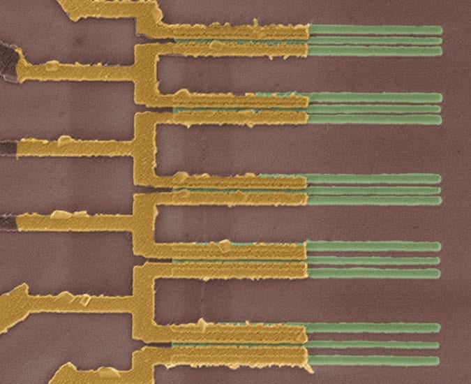
On Thursday, however, IBM scientists reported that they now believe they see a path around the wall. Writing in the journal Science, a team at the company’s Thomas J. Watson Research Center said it has found a new way to make transistors from parallel rows of carbon nanotubes.
The advance is based on a new way to connect ultrathin metal wires to the nanotubes that will make it possible to continue shrinking the width of the wires without increasing electrical resistance.
One of the principal challenges facing chip makers is that resistance and heat increase as wires become smaller, and that limits the speed of chips, which contain transistors.
The advance would make it possible, probably sometime after the beginning of the next decade, to shrink the contact point between the two materials to just 40 atoms in width, the researchers said. Three years later, the number will shrink to just 28 atoms, they predicted.
The ability to reduce electrical resistance will not only make it possible to extend the process of shrinking transistors beyond long-held beliefs about physical limits. It may also be the key to once again increasing the speed of computer processors, which has been stalled for the last decade.
The report represents a big advance for an exotic semiconductor material that has long held great promise but has also proved maddeningly difficult for scientists to work with. Single-wall carbon nanotubes are strawlike structures that are a composed of a one-atom thick matrix of carbon atoms rolled into an infinitesimally small tube.
The challenge of carbon nanotubes in their typical state is that they form what scientists call a giant “hairball” of interwoven molecules.
However, researchers have found ways to align them closely and in regularly spaced rows and deposit them on silicon wafers with great precision. They then serve the crucial role of a semiconductor, allowing electrical current to be switched on and off in a computer circuit.
Until now, however, they have been just one of a range of new materials that have been seen as candidates to replace silicon, which has for more than half a century been the material of choice for chip makers.
“Of all the possible materials, this one is at the top of the list by a long shot,” said Dario Gil, vice president for science and technology at IBM Research.
Read more: IBM Scientists Find New Way to Shrink Transistors
The Latest on: Transistors
[google_news title=”” keyword=”Transistors” num_posts=”10″ blurb_length=”0″ show_thumb=”left”]
via Google News
The Latest on: Transistors
- Insulated Gate Bipolar Transistors (IGBT) Industry Projected to Attain USD 14.9 Billion by 2033, Demonstrating an 8.3% CAGRon May 13, 2024 at 6:52 am
Market report, unveiled by Future Market Insights—an ESOMAR Certified Market Research and Consulting Firm—presents invaluable insights and meticulous analysis of the Insulated Gate Bipolar Transistors ...
- Nanowire Transistorson May 8, 2024 at 10:13 pm
Gupta, Manish and Kranti, Abhinav 2016. Transforming gate misalignment into a unique opportunity to facilitate steep switching in junctionless nanotransistors. Nanotechnology, Vol. 27, Issue. 45, p.
- Shockley diodes and their applicationson May 8, 2024 at 5:49 am
Diodes are fundamental building blocks in electronics, playing a vital role in controlling current flow, protecting circuits and enabling various functionalities. Because of their one-direction ...
- Exports Of Transistors Reached New High In Februaryon May 6, 2024 at 4:59 pm
EXPORTS of British transistors and phototransistors in February reached a new high level of over £76,000 in value,a 27 per cent increase on January's ...
- New memory transistor integrates photocrosslinker into molecular switches to adjust its threshold voltageon May 2, 2024 at 9:22 am
A research team has developed a memory transistor capable of adjusting its threshold voltage. This innovation combines two molecules that form a stable bond with a polymeric semiconductor, situated at ...
- “Magnetisation switching” can replace transistors, cutting energy demand from computing by an order of magnitudeon May 1, 2024 at 12:07 am
Globally, energy demand from computing is growing so fast the search is on to find fundamental ways to make it more efficient. “Magnetisation switching” has long been seen as a more efficient way than ...
- Organic electrochemical transistors: Scientists solve chemical mystery at the interface of biology and technologyon April 29, 2024 at 5:00 pm
Among those components are OECTs—or organic electrochemical transistors—which allow current to flow in devices like implantable biosensors. But scientists long knew about a quirk of OECTs that ...
- New transistors based on monolayer black phosphorus and germanium arsenideon January 6, 2024 at 5:32 am
"For a number of promising 2D materials—such as black phosphorus and germanium arsenide—the fabrication of monolayer transistors is challenging and is limited by the difficulties in forming ...
- CMOS Technology Explainedon April 29, 2023 at 7:36 am
CMOS technology combines two types of transistors that work together, leading to efficient power use and high noise immunity. CMOS technology uses two different types of transistors, n-type (nMOS) and ...
- Transistors explained – what they are and what they doon October 24, 2022 at 11:53 am
The impressive fact is that trillions of these transistors are integrated into electronic devices all over the Earth and even in space. The exterior layers of the transistor are known as the "drain" ...
via Bing News

