


Work could ultimately lead to electrical conductors that are 100 percent efficient
The future of electronics could lie in a material from its past, as researchers from The Ohio State University work to turn germanium—the material of 1940s transistors—into a potential replacement for silicon.
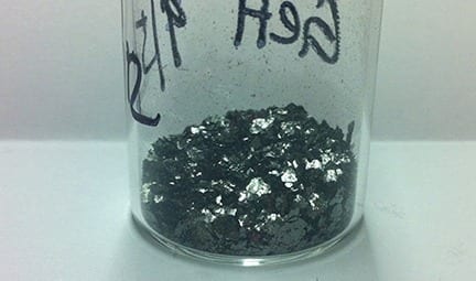
At the American Association for the Advancement of Science meeting, assistant professor of chemistry Joshua Goldberger reported progress in developing a form of germanium called germanane.
In 2013, Goldberger’s lab at Ohio State became the first to succeed at creating one-atom-thick sheet of germanane—a sheet so thin, it can be thought of as two-dimensional. Since then, he and his team have been tinkering with the atomic bonds across the top and bottom of the sheet, and creating hybrid versions of the material that incorporate other atoms such as tin.
The goal is to make a material that not only transmits electrons 10 times faster than silicon, but is also better at absorbing and emitting light—a key feature for the advancement of efficient LEDs and lasers.
“We’ve found that by tuning the nature of these bonds, we can tune the electronic structure of the material. We can increase or decrease the energy it absorbs,” Goldberger said. “So potentially we could make a material that traverses the entire electromagnetic spectrum, or absorbs different colors, depending on those bonds.”
As they create the various forms of germanane, the researchers are trying to exploit traditional silicon manufacturing methods as much as possible, to make any advancements easily adoptable by industry.
Aside from these traditional semiconductor applications, there have been numerous predictions that a tin version of the material could conduct electricity with 100 percent efficiency at room temperature.
Read more: The future of electronics—now in 2D

The Latest on: 2D electronics
[google_news title=”” keyword=”2D electronics” num_posts=”10″ blurb_length=”0″ show_thumb=”left”]
via Google News
The Latest on: 2D electronics
- Gesture Recognition And Touchless Sensing Market To Cross USD 104 Billion With Highest CAGR Of 9.51% By 2031on May 8, 2024 at 10:46 pm
The SNS Insider report highlights a promising future for the Gesture Recognition and Touchless Sensing Market , estimating it to reach USD 104 Billion by 2031. This growth signifies a CAGR of 9.51% ...
- EV batteries could last much longer thanks to new capacitor with 19-times energy density that scientists created by mistakeon May 8, 2024 at 3:00 am
Electric cars and laptop batteries could charge up much faster and last longer thanks to a new structure that can be used to make much better capacitors in the future.
- Researchers 'unzip' 2D materials with laserson May 7, 2024 at 8:42 am
In a new paper published on May 1 in the journal Science Advances, researchers at Columbia Engineering used commercially available tabletop lasers to create tiny, atomically sharp nanostructures, or ...
- Why researchers have created Goldene, a sheet of gold that is only one atom thickon May 6, 2024 at 11:06 pm
Creating ‘goldene’, as the one-atom thick material has been named, was not easy for the scientists behind the development, from Sweden’s Linköping University . It is not that such 2D materials have ...
- Columbia researchers “unzip” 2D materials with laserson May 6, 2024 at 4:59 pm
In a new paper in the journal Science Advances, researchers used commercially available tabletop lasers to create tiny, atomically sharp nanostructures in samples of a layered 2D material called ...
- Researchers create 2D all-organic perovskites, demonstrate potential use in 2D electronicson May 6, 2024 at 6:49 am
Perovskites are among the most researched topics in materials science. Recently, a research team from The Hong Kong Polytechnic University (PolyU) has solved an age-old challenge to synthesize ...
- The Hong Kong Polytechnic University: PolyU researchers create 2D all-organic perovskites and demonstrate potential use in 2D electronicson May 5, 2024 at 9:34 pm
Perovskites are among the most researched topics in materials science. Recently, a research team led by Prof. LOH Kian Ping, Chair Professor of Materials ...
- PolyU researchers create 2D all-organic perovskites and demonstrate potential use in 2D electronicson May 5, 2024 at 8:56 pm
Perovskites are named after their structural resemblance to the mineral calcium titanate perovskite, and are well known for their fascinating properties that can be applied in wide-ranging fields such ...
- The Novel Material Revolutionizing Energy Storageon April 28, 2024 at 10:00 am
Washington University in St. Louis scientists have developed a novel material that supercharges innovation in electrostatic energy storage, with the potential to revolutionize electronic devices.
- High-energy-density capacitors with 2D nanomaterials could significantly enhance energy storageon April 24, 2024 at 2:06 pm
In the quest for more efficient and sustainable energy solutions, a multi-university research team has reached a significant milestone in capacitor technology. Researchers from the University of ...
via Bing News

