


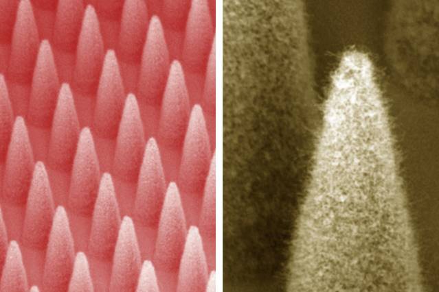
Image: Journal of Micrelectromechanical Systems/colorized by MIT News
Arrays of tiny conical tips that eject ionized materials could fabricate nanoscale devices cheaply
Luis Fernando Velásquez-García’s group at MIT’s Microsystems Technology Laboratories (MTL) develops dense arrays of microscopic cones that harness electrostatic forces to eject streams of ions.
The technology has a range of promising applications: depositing or etching features onto nanoscale mechanical devices; spinning out nanofibers for use in water filters, body armor, and “smart” textiles; or propulsion systems for fist-sized “nanosatellites.”
In the latest issue of the IEEE Journal of Microelectromechanical Systems, Velásquez-García, his graduate students Eric Heubel and Philip Ponce de Leon, and Frances Hill, a postdoc in his group, describe a new prototype array that generates 10 times the ion current per emitter that previous arrays did.
Ion current is a measure of the charge carried by moving ions, which translates directly to the rate at which particles can be ejected. Higher currents thus promise more-efficient manufacturing and more-nimble satellites.
The same prototype also crams 1,900 emitters onto a chip that’s only a centimeter square, quadrupling the array size and emitter density of even the best of its predecessors.
“This is a field that benefits from miniaturizing the components, because scaling down emitters implies less power consumption, less bias voltage to operate them, and higher throughput,” says Velásquez-García, a principal research scientist at MTL. “The topic we have been tackling is how we can make these devices operate as close as we can to the theoretical limit and how we can greatly increase the throughput by virtue of multiplexing, with massively parallel devices that operate uniformly.”
Nanoprinting
“In my opinion, the best nanosystems are going to be done by 3-D printing because it would bypass the problems of standard microfabrication,” Velásquez-García says. “It uses prohibitively expensive equipment, which requires a high level of training to operate, and everything is defined in planes. In many applications you want the three-dimensionality: 3-D printing is going to make a big difference in the kinds of systems we can put together and the optimization that we can do.”
Take me to the complete story . . .
The Latest on: Nanomanufacturing
[google_news title=”” keyword=”Nanomanufacturing” num_posts=”10″ blurb_length=”0″ show_thumb=”left”]
via Google News
The Latest on: Nanomanufacturing
- 3 startups awarded $200K through state’s Technology Validation Startup Fundon May 1, 2024 at 2:26 pm
The State of Ohio Technology Validation Startup Fund just awarded three tech startups $200,000 in grant awards. All three startups utilize technology developed at the ...
- Three McCormick Faculty Elected to American Academy of Arts and Scienceson April 26, 2024 at 10:09 am
Wei Chen, Mark C. Hersam, and Uri J. Wilensky are among the 250 members elected in 2024, and six from the University. They are recognized for their excellence and commitment to uphold the Academy’s ...
- Two-photon fabricationon April 5, 2024 at 1:29 am
As there is no other viable alternative to fully 3D nanomanufacturing, the expansion of 2PP as a production tool looks very promising. The sol–gel process is a relatively new material technology ...
- Ten things you should know about nanotechnologyon January 13, 2024 at 10:30 am
Of course, the chemical industry has long been working with nanoscale particles and pigments, but this falls more into the realm of chemistry than nanomanufacturing. Proponents of 'atomically precise ...
- New DNA nanobots can replicate themselves using UV lighton December 9, 2023 at 2:47 pm
"Our introduction of multiple-axis precise folding and positioning as a tool/technology for nanomanufacturing will open the door to more complex and useful nano- and microdevices," the team ...
- Nanomaterials Informationon January 19, 2022 at 10:07 am
Nanomaterials can also be engineered and are made through a process called nanomanufacturing. Nanomanufacturing has two basic approaches. Bottom-up builds products by building them up from atomic- and ...
- What is nanofabrication?on October 22, 2018 at 7:59 am
The terms nanofabrication and nanomanufacturing are used to describe the creation of functional and complex nanoscale structures in various industries, including medical, photonics, electronics, and ...
- Dr. Naoki Yokoyamaon August 29, 2018 at 10:31 am
For that reason, this Research Area solicits creative proposals for establishing nanomanufacturing technology that is meaningful in terms of engineering with new ideas based on nanoscale science.
- Nanomanufacturing Environmental Health and Safetyon March 2, 2017 at 5:48 am
Our mission is to ensure that students, faculty and staff in the nanomanufacturing laboratories are working safely, as well as (ii) to perform fundamental research on methods to measure and control ...
- Nanomanufacturing with Femtosecond Laser Irradiationson May 22, 2016 at 9:12 pm
A technique was recently found for fabricating nanostructures on a solid surface with intense femtosecond laser pulse irradiation. The technique is highly efficient because it is several orders faster ...
via Bing News

