


These new materials work well up to 100 GHz, opening the door for the next generation of devices for advanced communications.
Researchers from the National Institute of Standards and Technology (NIST) have joined with an international team to engineer and measure a potentially important new class of nanostructured materials for microwave and advanced communication devices. Based on NIST’s measurements, the new materials—a family of multilayered crystalline sandwiches—might enable a whole new class of compact, high-performance, high-efficiency components for devices such as cellular phones.
“These materials are an excellent example of what the Materials Genome Initiative refers to as ‘materials-by-design’,” says NIST physicist James Booth, one of the lead researchers. “Materials science is getting better and better at engineering complex structures at an atomic scale to create materials with previously unheard-of properties.”
The new multilayer crystals are so-called “tunable dielectrics,” the heart of electronic devices that, for example, enable cell phones to tune to a precise frequency, picking a unique signal out of the welter of possible ones.
Tunable dielectrics that work well in the microwave range and beyond—modern communications applications typically use frequencies around a few gigahertz—have been hard to make, according to NIST materials scientist Nathan Orloff. “People have created tunable microwave dielectrics for decades, but they’ve always used up way too much power.” These new materials work well up to 100 GHz, opening the door for the next generation of devices for advanced communications.
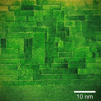
Modern cellphone dielectrics use materials that suffer from misplaced or missing atoms called “defects” within their crystal structure, which interfere with the dielectric properties and lead to power loss. One major feature of the new materials, says Orloff, is that they self-correct, reducing the effect of defects in the part of the crystal where it counts. “We refer to this material as having ‘perfect faults’,” he says. “When it’s being grown, one portion accommodates defects without affecting the good parts of the crystal. It’s able to correct itself and create perfect dielectric bricks that result in the rare combination of high tuning and low loss.”
The new material has layers of strontium oxide, believed to be responsible for the self-correcting feature, separating a variable number of layers of strontium titanate. Strontium titanate on its own is normally a pretty stable dielectric—not really tunable at all—but another bit of nanostructure wizardry solves that. The sandwich layers are grown as a thin crystalline film on top of a substrate material with a mismatched crystal spacing that produces strain within the strontium titanate structure that makes it a less stable dielectric—but one that can be tuned. “It’s like putting a queen-sized sheet on a king-sized bed,” says Orloff. “The combination of strain with defect control leads to the unique electronic properties.”
One key discovery by the research team was that, in addition to adding strain to the crystal sandwich, adding additional layers of strontium titanate in between the strontium oxide layers increased the room-temperature “tunability” performance of the structure, providing a new mechanism to control the material response. The material they reported on recently in the journal Nature has six layers of strontium titanate between each strontium oxide layer.
The new sandwich material performs so well as a tunable dielectric, over such a broad range of frequencies, that the NIST team led by Booth had to develop a new measurement technique—an array of test structures fabricated on top of the test film—just to measure its electronic characteristics. “We were able to characterize the performance of these materials as a function of frequency running from 10 hertz all the way up to 125 gigahertz. That’s the equivalent of measuring wavelengths from kilometers down to microns all with the same experimental set-up,” says Orloff, adding, “This material has a much lower loss and a much higher tunability for a given applied field then any material that we have seen.”
Go deeper with Bing News on:
Tunable dielectrics
- Breakthroughs in optical modulation using tunable 2D materials
This capability is attributed to the tunable electrical conduction arising from the reversible migration of mobile Cu ions at the metal-semiconductor interface. The flexibility of the Cu–S bond ...
- New Approach to Designing Advanced Dielectrics
In a recent study published in the journal Dalton Transactions, scientists at the Shibaura Institute of Technology have made significant progress in the creation of displacement-type ferroelectric ...
- The New, Tunable Gen-4 Coyote Crate Engine Keeps Hot Rodding Alive
Ford has addressed the V-8 community's demands by offering a pair of re-vamped Gen 4 Coyote crate engines, both of which turn the power up to MAX. Ford Performance's Coyote V-8 engines offer power ...
- The Benefits of Tunable White Light
Today, tunable white lights offer a reliable technology that can help create an environment that supports alertness and productivity by helping workers maintain their natural circadian rhythm (Photo 1 ...
- Meta-Optics: Pushing the Boundaries of Light Manipulation
The development of active and tunable meta-optical components, such as electrically or optically controlled metasurfaces, will enable dynamic control over light manipulation. The exploration of new ...
Go deeper with Google Headlines on:
Tunable dielectrics
[google_news title=”” keyword=”Tunable dielectrics” num_posts=”5″ blurb_length=”0″ show_thumb=”left”]
Go deeper with Bing News on:
Nanostructured materials
- 12 types of roofing materials: Guide to choosing the best ones for you
Depending on what factors matter to you, different types of roofing materials like metal, solar, clay or slate might be attractive alternatives with their own advantages to offer. Get free ...
- Seven faculty members elected AAAS Fellows
Seven UT faculty members have been elected to the latest class of fellows for the American Association for the Advancement of Science, a distinguished lifetime honor within the scientific community.
- Bio-inspired materials' potential for efficient mass transfer boosted by a new twist on a century-old theory
The natural vein structure found within leaves -- which has inspired the structural design of porous materials that can maximize mass transfer -- could unlock improvements in energy storage, catalysis ...
- Researchers establish commercially viable process for manufacturing with promising new class of metals
Nanostructured high entropy alloys—metals made from a chaotic mix of several different elements—show a lot of promise for use in industries such as aerospace and automotive because of their strength ...
- X-ray study offers first look at a quantum version of the liquid-crystal phase
A team of scientists, with help from Argonne National Laboratory’s Advanced Photon Source, have demonstrated the existence of an elusive state of matter known as quantum spin nematic.
Go deeper with Google Headlines on:
Nanostructured materials
[google_news title=”” keyword=”nanostructured materials” num_posts=”5″ blurb_length=”0″ show_thumb=”left”]

