


“Open-innovation is key to move from early-stage precompetitive technology to the development of robust products such as these next-generation medical devices.”
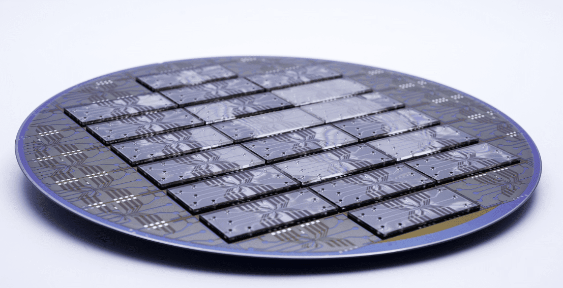
Imec, a world-leading nanoelectronics research center and JSR, a leading materials company, announce that they have successfully used JSR’s innovative PA (Photo-patternable Adhesive) material for wafer-scale processing of lab-on-chip devices. With PA as a key enabling material, imec has processed microfluidic cell-sorter devices, merging microheaters and sensors with wafer-scale polymer microfluidics. PA is a breakthrough material: a good microfluidic channel material and adhesive at the same time, suitable for wafer-scale processes and mass production.
Lab-on-chip technology will drive a revolution in medical technology in the years to come. It will enable powerful point-of-care diagnosis and treatment through on-chip molecular synthesis, separation, sensing, and detection. Key will be the ability to integrate microfluidics with heterogeneous components such as electronics, sensors, microheaters, and photonics in a cost-effective manner. To merge these elements successfully, new bonding and surface treatment materials are needed.
“PA solves a number of issues that we have with other materials, such as the widely-used PDMS (polydimethylsiloxane, a silicon-based organic polymer)”, says Liesbet Lagae, imec R&D manager of life science technologies. It has all the characteristics we are looking for in a photopatternable material to create microfluidic channels on silicon wafers, including a good channel definition and biocompatibility. But at the same time, it is an adhesive that allows direct thermal bonding with the cover glass. And unlike PDMS, it allows for wafer-scale processing, which is a prerequisite for industrial mass production.”
Imec used PA to process the next generation of its cell sorter lab-on-chip. Integrating on-chip imaging, in-flow cell tomography to identify cells, and bubble jet-flow technology to guide and sort individual cells, the prototype lab-on-chip can process up to 2,000 cells per second. One application envisaged for these ultrafast cell-sorters is the detection of circulating tumor cells in human blood.

Go deeper with Bing News on:
Mass production of lab-on-chip
- Rapidus gears up for advanced packaging and chiplet technologies as it races to 2nm production
Japan's semiconductor foundry startup Rapidus, now on a mission to mass produce 2nm chips by 2027, is developing advanced packaging and chiplet technologies, with a particular focus on interposer ...
- AI chip startup DEEPX secures $80M Series C at a $529M valuation
The Series C funding, which brings its total raise to around $95 million, will go toward mass production of the startup's inaugural products ...
- Q&A: How advanced chip packaging can help redesign the future of semiconductors
The phrase "advanced chip packaging" might conjure images of a fancy Pringles can. For those who manufacture semiconductors—also known as integrated circuits, chips or microchips—it represents a new ...
- Samsung's first 3nm Exynos chip nears mass production phase
Samsung has announced it is almost ready to enter mass production for its 3nm process chip, which could happen in the next few months.
- Rapidus Gearing Up for Mass Production of Next-Generation Chips
Tokyo, May 6 (Jiji Press)--Japan's Rapidus Corp. is stepping up efforts to embark on mass production ... domestic production of state-of-the-art semiconductors. Reviving the Japanese chip industry ...
Go deeper with Google Headlines on:
Mass production of lab-on-chip
[google_news title=”” keyword=”Mass production of lab-on-chip” num_posts=”5″ blurb_length=”0″ show_thumb=”left”]
Go deeper with Bing News on:
Lab on a chip
- Congress must face the greatest ‘risk’ in the chips war head-on
But one of the biggest issues Congress faces is something you may have never heard of. It’s RISC-V, or “risk five,” a chip design technology and a key ingredient in producing advanced chips that power ...
- Elon Musk’s first Neuralink brain chip patient encountered a problem after implant surgery, scientists reveals
ELON Musk's controversial brain chip lab Neuralink has revealed their first ever patient experienced an issue after surgery. Noland Arbaugh, 29, who is paralysed from the neck down, received the ...
- Q&A: How advanced chip packaging can help redesign the future of semiconductors
The phrase "advanced chip packaging" might conjure images of a fancy Pringles can. For those who manufacture semiconductors—also known as integrated circuits, chips or microchips—it represents a new ...
- Grounded: How To Get The Haze Lab BURGL Chip
Obtaining the BURG.L chip from the Haze Lab in Grounded requires players to complete a few steps before claiming the prize. Your browser does not support the video ...
- New diagnostic tool achieves accuracy of PCR tests with faster and simpler nanopore system
The nanopore optofluidic chip used in the new diagnostic system, with a PCR thermocycler in the background for comparison. The new system could easily fit into a researcher’s lab or clinician ...
Go deeper with Google Headlines on:
Lab on a chip
[google_news title=”” keyword=”lab on a chip” num_posts=”5″ blurb_length=”0″ show_thumb=”left”]

