


University of Washington scientists have built a new nanometer-sized laser — using the thinnest semiconductor available today — that is energy efficient, easy to build and compatible with existing electronics.
Lasers play essential roles in countless technologies, from medical therapies to metal cutters to electronic gadgets. But to meet modern needs in computation, communications, imaging and sensing, scientists are striving to create ever-smaller laser systems that also consume less energy.
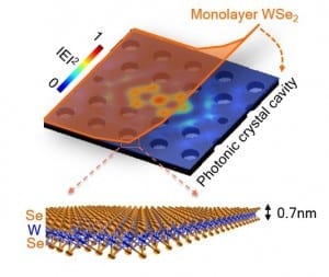
The UW nanolaser, developed in collaboration with Stanford University, uses a tungsten-based semiconductor only three atoms thick as the “gain material” that emits light. The technology is described in a paper published in the March 16 online edition of Nature.
“This is a recently discovered, new type of semiconductor which is very thin and emits light efficiently,” said Sanfeng Wu, lead author and a UW doctoral candidate in physics. “Researchers are making transistors, light-emitting diodes, and solar cells based on this material because of its properties. And now, nanolasers.”
Nanolasers — which are so small they can’t be seen with the eye — have the potential to be used in a wide range of applications from next-generation computing to implantable microchips that monitor health problems. But nanolasers so far haven’t strayed far from the research lab.
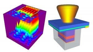
Other nanolaser designs use gain materials that are either much thicker or that are embedded in the structure of the cavity that captures light. That makes them difficult to build and to integrate with modern electrical circuits and computing technologies.
The UW version, instead, uses a flat sheet that can be placed directly on top of a commonly used optical cavity, a tiny cave that confines and intensifies light. The ultrathin nature of the semiconductor — made from a single layer of a tungsten-based molecule — yields efficient coordination between the two key components of the laser.
The UW nanolaser requires only 27 nanowatts to kickstart its beam, which means it is very energy efficient.
Other advantages of the UW team’s nanolaser are that it can be easily fabricated, and it can potentially work with silicon components common in modern electronics. Using a separate atomic sheet as the gain material offers versatility and the opportunity to more easily manipulate its properties.
“You can think of it as the difference between a cell phone where the SIM card is embedded into the phone versus one that’s removable,” said co-author Arka Majumdar, UW assistant professor of electrical engineering and of physics.
“When you’re working with other materials, your gain medium is embedded and you can’t change it. In our nanolasers, you can take the monolayer out or put it back, and it’s much easier to change around,” he said.
The researchers hope this and other recent innovations will enable them to produce an electrically-driven nanolaser that could open the door to using light, rather than electrons, to transfer information between computer chips and boards.
Read more: UW scientists build a nanolaser using a single atomic sheet
The Latest on: Nanolaser
[google_news title=”” keyword=”Nanolaser” num_posts=”10″ blurb_length=”0″ show_thumb=”left”]
via Google News
The Latest on: Nanolaser
- Birth of the nanolaseron April 6, 2024 at 3:25 pm
Interestingly, the two nanolaser designs reported in Nature are strikingly different. The approach of Noginov et al. is to use a spherical cavity — a composite 44-nm-diameter nanoparticle (lower ...
- Nanolasers: Miniaturized Light Sources for Advanced Applicationson March 20, 2024 at 3:15 am
Optical Cavity: The optical cavity provides the necessary feedback for light amplification in a nanolaser. It confines the light emitted by the gain medium, allowing for multiple passes through the ...
- Nanowire photonicson November 30, 2021 at 12:28 pm
Despite all the progress made in optically pumped nanowire lasing, realization of a reliable, electrically injected nanowire nanolaser 66 remains a major challenge, owing to issues such as the ...
via Bing News
