Graphene-based device could accelerate the development of 2D photoelectronics
The Center for Integrated Nanostructure Physics, within the Institute for Basic Science (IBS) has developed the world’s thinnest photodetector, that is a device that converts light into an electric current. With a thickness of just 1.3 nanometers – 10 times smaller than the current standard silicon diodes – this device could be used in the Internet of Things, smart devices, wearable electronics and photoelectronics. This 2D technology, published on Nature Communications, uses molybdenum disulfide (MoS2) sandwiched in graphene.
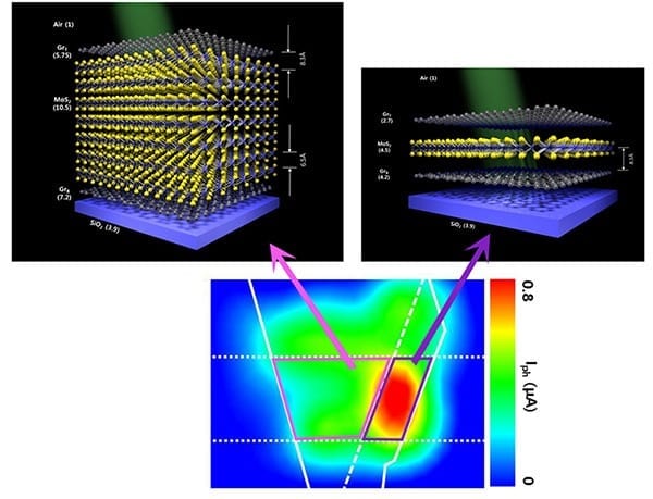
Graphene is a fantastic material: It’s conductive, thin (just one-atom thick), transparent and flexible. However, since it does not behave as a semiconductor, its application in the electronics industry is limited. Therefore, in order to increase graphene’s usability, IBS scientists sandwiched a layer of the 2D semiconductor MoS2 between two graphene sheets and put it over a silicon base. They initially thought the resulting device was too thin to generate an electric current but, unexpectedly, it did. “A device with one-layer of MoS2 is too thin to generate a conventional p-n junction, where positive (p) charges and negative (n) charges are separated and can create an internal electric field. However, when we shine light on it, we observed high photocurrent. It was surprising! Since it cannot be a classical p-n junction, we thought to investigate it further,” explains YU Woo Jong, first author of this study.
To understand what they found, the researchers compared devices with one and seven layers of MoS2 and tested how well they behave as a photodetector, that is, how they are able to convert light into an electric current. They found that the device with one-layer MoS2 absorbs less light than the device with seven layers, but it has higher photoresponsitivity. “Usually the photocurrent is proportional to the photoabsorbance, that is, if the device absorbs more light, it should generate more electricity, but in this case, even if the one-layer MoS2 device has smaller absorbance than the seven-layer MoS2, it produces seven times more photocurrent,” describes Yu.
Why is the thinner device working better than the thicker one? The research team proposed a mechanism to explain why this is the case. They recognized that the photocurrent generation could not be explained with classical electromagnetism, but could be with quantum physics. When light hits the device, some electrons from the MoS2 layer jump into an excited state and their flow through the device produces an electric current. However in order to pass the boundary between MoS2 and graphene, the electrons need to overcome an energy barrier (via quantum tunnelling), and this is where the one-layer MoS2 device has an advantage over the thicker one.
The monolayer is thinner and therefore more sensitive to the surrounding environment: The bottom SiO2 layer increases the energy barrier, while the air on top reduces it, thus electrons in the monolayer device have a higher probability to tunnel from the MoS2 layer to the top graphene (GrT). The energy barrier at the GrT/MoS2 junction is lower than the one at the GrB/MoS2, so the excited electrons transfer preferentially to the GrT layer and create an electric current. Conversely, in the multi-layer MoS2 device, the energy barriers between GrT/MoS2 and GrB/MoS2 are symmetric, therefore the electrons have the same probability to go either side and thus reduce the generated current.
Imagine a group of people in a valley surrounded by two mountains. The group wants to get to the other side of the mountains, but without making too much effort. In one case ( the seven-layers MoS2 device), both mountains have the same height so whichever mountain is crossed, the effort will be the same. Therefore half the group crosses one mountain and the other half the second mountain.
In the second case (analogue to the one-layer MoS2 device), one mountain is taller than the other, so the majority of the group decide to cross the smaller mountain. However, because we are considering quantum physics instead of classical electromagnetism, they do not need to climb the mountain until they reach the top (as they would need to do with classical physics), but they can pass through a tunnel. Although electron tunneling and walking a tunnel in a mountain are very different of course, the idea is that electric current is generated by the flow of electrons, and the thinner device can generate more current because more electrons flow towards the same direction.
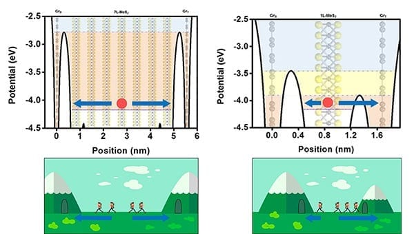
(top) In the one-layer device MoS2 (right), the electron (red circle) has a higher probability to tunnel from the MoS2 layer to the GrT because the energy barrier (white arch) is smaller in that junction. In the seven-layers MoS2 device (left) instead, the energy barrier between MoS2/GrT and MoS2/GrB is the same so electrons do not have a preferred direction flow. More energy is generated in the one-layer MoS2 device because more electrons flow in the same direction.
(bottom) Imagine that people want to cross a mountain without too much effort. If the mountains have different height (right), more people choose to climb (or better, to tunnel) the small mountain, while if the mountains have the same height (left), they do not have a preferred route. (Graphics modified from Freepiks)
Actually, when light is absorbed by the device and MoS2 electrons jump into an excited state, they leave the so-called holes behind. Holes behave like positive mobile charges and are essentially positions left empty by electrons that absorbed enough energy to jump to a higher energy status. Another problem of the thicker device is that electrons and holes move too slowly through the junctions between graphene and MoS2, leading to their undesired recombination within the MoS2 layer.
For these reasons, up to 65% of photons absorbed by the thinner device are used to generate a current. Instead, the same measurement (quantum efficiency) is only 7% for the seven-layer MoS2 apparatus.
“This device is transparent, flexible and requires less power than the current 3D silicon semiconductors. If future research is successful, it will accelerate the development of 2D photoelectric devices,” explains the professor.
Learn more: The Thinnest Photodetector in the World
The Latest on: 2D photoelectronics
[google_news title=”” keyword=”2D photoelectronics” num_posts=”10″ blurb_length=”0″ show_thumb=”left”]
via Google News
The Latest on: 2D photoelectronics
- Atom-by-atom: Imaging structural transformations in 2D materialson April 17, 2024 at 2:53 pm
Two-dimensional (2D) materials have a rich array of properties, including superconductivity and magnetism, and are promising candidates for use in electronic systems, such as transistors.
- Goldene: New 2D form of gold makes graphene look boringon April 17, 2024 at 12:29 am
The researchers say that goldene gets its new properties because in its 2D form, the atoms get two “free bonds.” This means it could eventually find use as a catalyst for converting carbon ...
- Inti Creates announces fantasy robot anime-inspired 2D action game Divine Dynamo Flamefriton March 31, 2024 at 8:01 am
Explore a Fantasy World Filled Swords and Magic! Today, April 1, 2024, April Fools’ Day*, Inti Creates has announced development on a new 2D action adventure game, Divine Dynamo Flamefrit.
- This Fascinating Indie Game Requires You To Simultaneously Play In 2D And 3Don March 28, 2024 at 5:16 pm
The game allows players to simultaneously control their character in a 2D and 3D. Screenbound, an upcoming indie game on Steam, is gaining attention for its unique premise. The developers describe ...
- Concepts and Methods of 2D Infrared Spectroscopyon February 26, 2023 at 10:38 pm
Laaser, Jennifer E. Xiong, Wei and Zanni, Martin T. 2011. Time-Domain SFG Spectroscopy Using Mid-IR Pulse Shaping: Practical and Intrinsic Advantages. The Journal of ...
- 2D and 3D shapeson August 16, 2020 at 11:21 pm
Explore the properties of 2D shapes from one-sided circles to the eight-sided octagons. Shapes with 3 sides Explore shapes with 3 sides and look at curved and straight lines. Shapes with 4 sides ...
- What are 2D shapes?on July 25, 2020 at 9:11 pm
These guys are 2D shapes and 2D shapes are everywhere. Shapes have sides and corners and are completely flat, like a drawing on a piece of paper. Circles don’t have corners and have got just one ...
- Graphene and 2D materials could move electronics beyond ‘Moore’s Law’on June 3, 2020 at 7:42 am
Recent theoretical and experimental advances and phenomena in studies of electronic spin transport in graphene and related two-dimensional (2D) materials have emerged as a fascinating area of research ...
- 2D polymerson August 25, 2018 at 6:38 pm
The properties of 2D materials, such as graphene, arise not only from their composition but also their sheet-like structures. Synthetic 2D polymers made from well-defined monomers promise to ...
via Bing News

