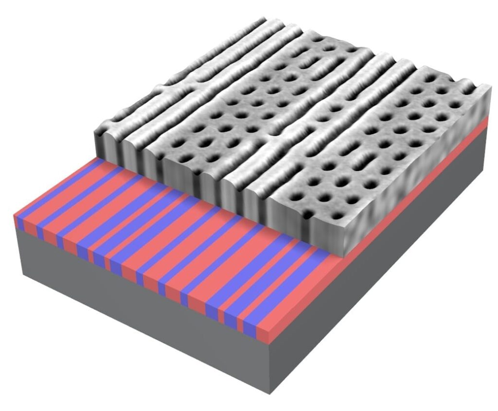
Brookhaven Lab scientists discover a way to create billionth-of-a-meter structures that snap together in complex patterns with unprecedented efficiency
To continue advancing, next-generation electronic devices must fully exploit the nanoscale, where materials span just billionths of a meter. But balancing complexity, precision, and manufacturing scalability on such fantastically small scales is inevitably difficult. Fortunately, some nanomaterials can be coaxed into snapping themselves into desired formations—a process called self-assembly.
Scientists at the U.S. Department of Energy’s (DOE) Brookhaven National Laboratory have just developed a way to direct the self-assembly of multiple molecular patterns within a single material, producing new nanoscale architectures. The results were published in the journal Nature Communications.
“This is a significant conceptual leap in self-assembly,” said Brookhaven Lab physicist Aaron Stein, lead author on the study. “In the past, we were limited to a single emergent pattern, but this technique breaks that barrier with relative ease. This is significant for basic research, certainly, but it could also change the way we design and manufacture electronics.”
Microchips, for example, use meticulously patterned templates to produce the nanoscale structures that process and store information. Through self-assembly, however, these structures can spontaneously form without that exhaustive preliminary patterning. And now, self-assembly can generate multipledistinct patterns—greatly increasing the complexity of nanostructures that can be formed in a single step.
“This technique fits quite easily into existing microchip fabrication workflows,” said study coauthor Kevin Yager, also a Brookhaven physicist. “It’s exciting to make a fundamental discovery that could one day find its way into our computers.”
The experimental work was conducted entirely at Brookhaven Lab’s Center for Functional Nanomaterials (CFN), a DOE Office of Science User Facility, leveraging in-house expertise and instrumentation.
Cooking up organized complexity
The collaboration used block copolymers—chains of two distinct molecules linked together—because of their intrinsic ability to self-assemble.
“As powerful as self-assembly is, we suspected that guiding the process would enhance it to create truly ‘responsive’ self-assembly,” said study coauthor Greg Doerk of Brookhaven. “That’s exactly where we pushed it.”
Learn more: Smarter Self-assembly Opens New Pathways for Nanotechnology
The Latest on: Self-assembly
[google_news title=”” keyword=”self-assembly” num_posts=”10″ blurb_length=”0″ show_thumb=”left”]
via Google News
The Latest on: Self-assembly
- General Assembly discusses Palestine's failed UN membership bidon May 3, 2024 at 12:41 pm
Palestine’s recent attempt to become a full member of the United Nations was the focus of discussion in the General Assembly on Wednesday.
- Obuasi East District Assembly inaugurates Town Councilson May 3, 2024 at 12:19 pm
The Obuasi East District Assembly has inaugurated three Town Councils, namely: Wawasi-Kwabrafoso Town Council, Tutuka-Odumasi Town Council and Brahabebome-Akaporiso Town Council to help the Assembly ...
- United Methodists remove LGBTQ+ funding ban in step toward more inclusive churchon April 30, 2024 at 1:02 pm
On the second day of the final week of the UMC General Conference in Charlotte, delegates passed petitions seeking to remove anti-LGBTQ+ restrictions.
- New class of spongy materials can self-assemble into precisely controllable structureson April 30, 2024 at 8:02 am
A team of researchers led by the University of Massachusetts Amherst has drawn inspiration from a wide variety of natural geometric motifs—including those of 12-sided dice and potato chips—in order to ...
- Kentucky General Assembly fumbles opportunities to help kidson April 30, 2024 at 2:02 am
Kentucky General Assembly had a chance to helps kids and during session, instead they missed opportunities, says Kentucky youth advocate Terry Brooks ...
- Scientists construct sophisticated synthetic system using self-replicating nanostructureson April 29, 2024 at 7:03 am
A research team led by the late Professor Liang Haojun from the Hefei National Laboratory for Physical Sciences at the Microscale of University of Science and Technology of China (USTC) has developed ...
- Aird rips Petersburg's casino pick, blasts council for choosing self-service over serving citizenson April 26, 2024 at 9:40 pm
Petersburg's state senator claims City Council's decision to go with former collaborator is an example of its 'ongoing struggle' to govern in its citizens' best interests ...
- Scientists learn from caterpillars how to create self-assembling capsules for drug deliveryon April 26, 2024 at 8:00 am
Self-assembling molecules that spontaneously organize themselves to form complex structures are common in nature. For example, the tough outer layer of insects, called the cuticle, is rich in proteins ...
- General Assembly debates Security Council’s rising veto useon April 23, 2024 at 11:24 am
The General Assembly on Tuesday debated veto power in the Security Council on the eve of the second anniversary of a special measure adopted to monitor its use, following on the heels of the United ...
- The right to assembly is now in jeopardy. This why you should be concernedon April 21, 2024 at 2:15 pm
Last week, the Supreme Court effectively abolished the right to assembly in three Southern states. By refusing to hear an appeal of a speaker accused of being liable for what a protester did in an ...
via Bing News

