


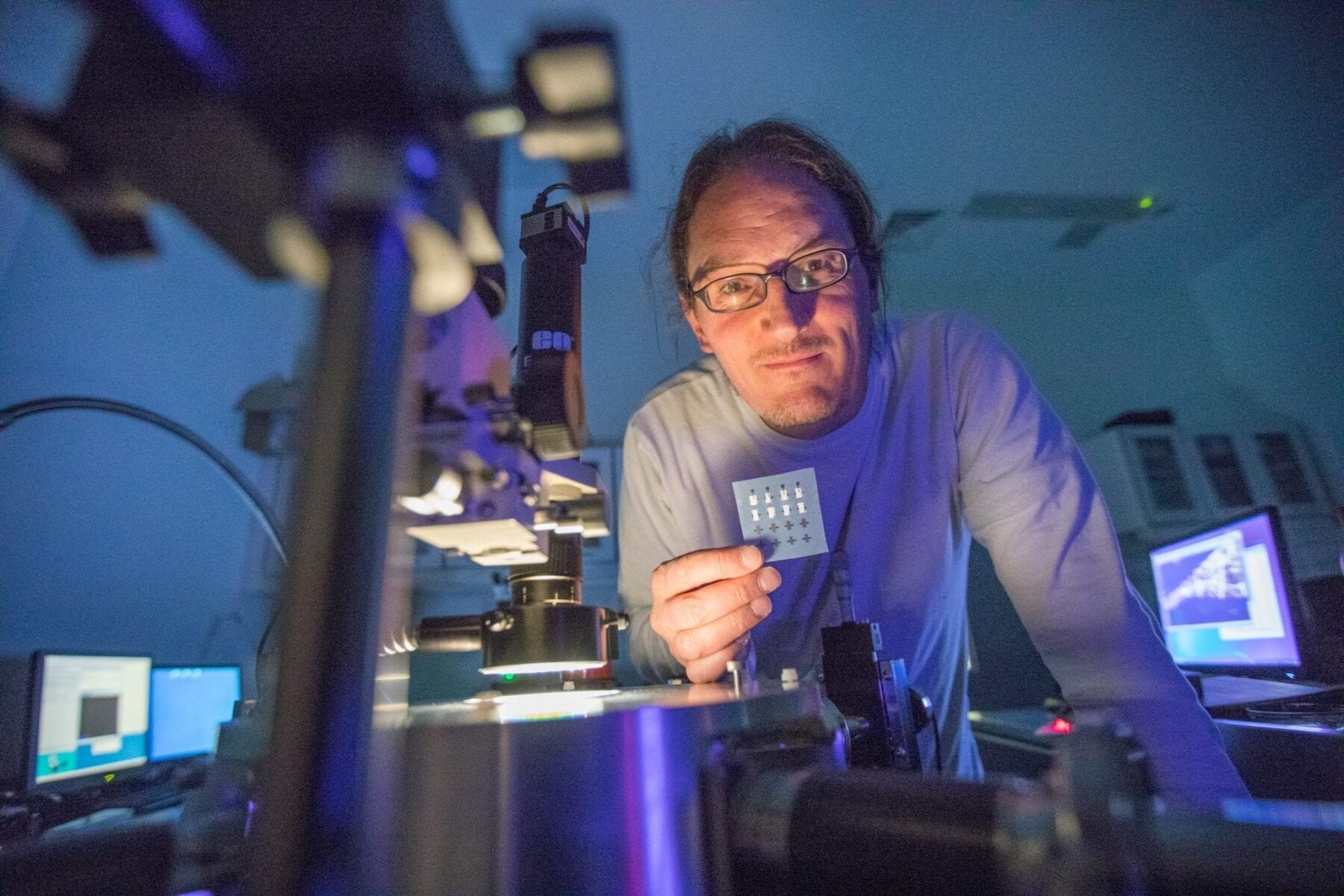

Scientists in AMBER, the Science Foundation Ireland-funded materials science research centre hosted in Trinity College Dublin, have fabricated printed transistors consisting entirely of 2-dimensional nanomaterials for the first time.
These 2D materials combine exciting electronic properties with the potential for low-cost production. This breakthrough could unlock the potential for applications such as food packaging that displays a digital countdown to warn you of spoiling, wine labels that alert you when your white wine is at its optimum temperature, or even a window pane that shows the day’s forecast.
The AMBER team’s findings have just been published today in the leading journal Science.
This discovery opens the path for industry, such as ICT and pharmaceutical, to cheaply print a host of electronic devices from solar cells to LEDs with applications from interactive smart food and drug labels to next-generation banknote security and e-passports.
Professor of Chemical Physics at Trinity, Jonathan Coleman, who is an investigator in AMBER, said: “In the future, printed devices will be incorporated into even the most mundane objects such as labels, posters and packaging. Printed electronic circuitry (constructed from the devices we have created) will allow consumer products to gather, process, display and transmit information: for example, milk cartons could send messages to your phone warning that the milk is about to go out-of-date.
We believe that 2D nanomaterials can compete with the materials currently used for printed electronics. Compared to other materials employed in this field, our 2D nanomaterials have the capability to yield more cost effective and higher performance printed devices. However, while the last decade has underlined the potential of 2D materials for a range of electronic applications, only the first steps have been taken to demonstrate their worth in printed electronics. This publication is important because it shows that conducting, semiconducting and insulating 2D nanomaterials can be combined together in complex devices. We felt that it was critically important to focus on printing transistors as they are the electric switches at the heart of modern computing. We believe this work opens the way to print a whole host of devices solely from 2D nanosheets.”
Led by Professor Coleman, in collaboration with the groups of Professor Georg Duesberg (AMBER) and Professor Laurens Siebbeles (TU Delft, Netherlands), the team used standard printing techniques to combine graphene nanosheets as the electrodes with two other nanomaterials — tungsten diselenide and boron nitride — as the channel and separator (two important parts of a transistor) to form an all-printed, all-nanosheet, working transistor.
Printable electronics have developed over the last 30 years based mainly on printable carbon-based molecules. While these molecules can easily be turned into printable inks, such materials are somewhat unstable and have well-known performance limitations.
There have been many attempts to surpass these obstacles using alternative materials, such as carbon nanotubes or inorganic nanoparticles, but these materials have also shown limitations in either performance or in manufacturability. While the performance of printed 2D devices cannot yet compare with advanced transistors, the team believe there is a wide scope to improve performance beyond the current state of the art for printed transistors.
The ability to print 2D nanomaterials is based on Professor Coleman’s scalable method of producing 2D nanomaterials, including graphene, boron nitride, and tungsten diselenide nanosheets, in liquids — a method he has licensed to Samsung and Thomas Swan. These nanosheets are flat nanoparticles that are a few nanometres thick but hundreds of nanometres wide.
Critically, nanosheets made from different materials have electronic properties that can be conducting, insulating or semiconducting and so include all the building blocks of electronics. Liquid processing is especially advantageous in that it yields large quantities of high quality 2D materials in a form that is easy to process into inks. Professor Coleman’s publication provides the potential to print circuitry at extremely low cost, which will facilitate a range of applications from animated posters to smart labels.
Learn more: Scientists make major breakthrough in smart printed electronics

[osd_subscribe categories=’printed-electronics-2′ placeholder=’Email Address’ button_text=’Subscribe Now for any new posts on the topic “PRINTED ELECTRONICS”‘]
The Latest on: Printed electronics
[google_news title=”” keyword=”printed electronics” num_posts=”10″ blurb_length=”0″ show_thumb=”left”]
via Google News
The Latest on: Printed electronics
- Scientists claim ‘breakthrough’ separating plastics from e-scrapon April 26, 2024 at 7:18 am
Dutch tech research institute TNO has developed a new method it says could drastically transform the landscape of electronics recycling. With an ...
- Easy EKG for a Chimpanzeeon April 25, 2024 at 5:00 pm
One mechanical problem remained, though: The electronics housed at the center of the bar were not well-protected. In fact, the 3D-printed electronics housing had been chewed through (but not eaten) by ...
- Warm Windows and Streamlined Skin Patches – IDTechEx Explores Flexible and Printed Electronicson April 25, 2024 at 5:00 pm
Flexible and printed electronics can be integrated into cars and homes to create modern aesthetics that are beneficial and easy to use. From luminous car controls to food labels that communicate the ...
- IDTechEx Report Unveils 3D Electronics Status and Opportunitieson April 21, 2024 at 11:32 pm
D electronics is an emerging manufacturing approach that enables electronics to be integrated within or onto the surface of objects. 3D electronic manufacturing techniques empower new features, ...
- Vietnam Printed Electronics Market Latest Trends, Segmentation Analysis, Share, Size, and Forecast 2024 to 2032on April 17, 2024 at 3:09 pm
The recent analysis by Report Ocean on the “Vietnam Printed Electronics Market” Report 2024 to 2032 revolves around various aspects of the market, including characteristics, size and growth, ...
- IDTechEx Release New Global 3D Electronics Market Reporton April 12, 2024 at 6:35 am
BOSTON, April 12, 2024 IDTechEx Research, a trusted provider of independent market intelligence, announces the availability of a new report, "3D Electronics/Additive Electronics 2024-2034: ...
- Customized silicon chips for material characterization of printed electronicson March 27, 2024 at 11:57 am
Organic semiconductors are key components in organic electronics and photovoltaics. They are used to make flexible electronic devices and printed solar cells. Typical for this class of materials ...
- 3d printed electronicson October 1, 2023 at 5:00 pm
This modular coil is intended to be used in motor and generator applications, and features a 3D printed structure to wind your copper about as well as a series of ferromagnetic machine screws and ...
- Printed Electronics Researchon August 17, 2020 at 2:31 am
The core mission of PERC is to develop new devices and subsystems that provide electromagnetic, electronic and photonic functionality using Additive Manufacturing and Printed Electronics approaches.
via Bing News

