As far back as the 1990s, long before anyone had actually isolated graphene — a honeycomb lattice of carbon just one atom thick — theorists were predicting extraordinary properties at the edges of graphene nanoribbons.
Now physicists at the U.S. Department of Energy’s Lawrence Berkeley National Laboratory (Berkeley Lab), and their colleagues at the University of California at Berkeley, Stanford University, and other institutions, have made the first precise measurements of the “edge states” of well-ordered nanoribbons.
A graphene nanoribbon is a strip of graphene that may be only a few nanometers wide (a nanometer is a billionth of a meter). Theorists have envisioned that nanoribbons, depending on their width and the angle at which they are cut, would have unique electronic, magnetic, and optical features, including band gaps like those in semiconductors, which sheet graphene doesn’t have.
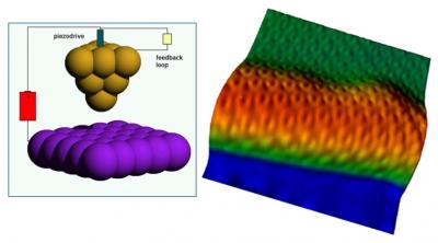
“Until now no one has been able to test theoretical predictions regarding nanoribbon edge-states, because no one could figure out how to see the atomic-scale structure at the edge of a well-ordered graphene nanoribbon and how, at the same time, to measure its electronic properties within nanometers of the edge,” says Michael Crommie of Berkeley Lab’s Materials Sciences Division (MSD) and UC Berkeley’s Physics Division, who led the research. “We were able to achieve this by studying specially made nanoribbons with a scanning tunneling microscope.”
The team’s research not only confirms theoretical predictions but opens the prospect of building quick-acting, energy-efficient nanoscale devices from graphene-nanoribbon switches, spin-valves, and detectors, based on either electron charge or electron spin. Farther down the road, graphene nanoribbon edge states open the possibility of devices with tunable giant magnetoresistance and other magnetic and optical effects.


