


A new method to produce large, monolayer single-crystal-like graphene films more than a foot long relies on harnessing a “survival of the fittest” competition among crystals. The novel technique, developed by a team led by the Department of Energy’s Oak Ridge National Laboratory, may open new opportunities for growing the high-quality two-dimensional materials necessary for long-awaited practical applications.
Making thin layers of graphene and other 2D materials on a scale required for research purposes is common, but they must be manufactured on a much larger scale to be useful.
Graphene is touted for its potential of unprecedented strength and high electrical conductivity and can be made through well-known approaches: separating flakes of graphite—the silvery soft material found in pencils—into one-atom-thick layers, or growing it atom by atom on a catalyst from a gaseous precursor until ultrathin layers are formed.
The ORNL-led research team used the latter method—known as chemical vapor deposition, or CVD—but with a twist. In a study published in Nature Materials, they explained how localized control of the CVD process allows evolutionary, or self-selecting, growth under optimal conditions, yielding a large, single-crystal-like sheet of graphene.
“Large single crystals are more mechanically robust and may have higher conductivity,” ORNL lead coauthor Ivan Vlassiouk said. “This is because weaknesses arising from interconnections between individual domains in polycrystalline graphene are eliminated.”
“Our method could be the key not only to improving large-scale production of single-crystal graphene but to other 2D materials as well, which is necessary for their large-scale applications,” he added.
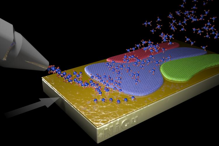
Much like traditional CVD approaches to produce graphene, the researchers sprayed a gaseous mixture of hydrocarbon precursor molecules onto a metallic, polycrystalline foil. However, they carefully controlled the local deposition of the hydrocarbon molecules, bringing them directly to the edge of the emerging graphene film. As the substrate moved underneath, the carbon atoms continuously assembled as a single crystal of graphene up to a foot in length.
“The unencumbered single-crystal-like graphene growth can go almost continuously, as a roll-to-roll and beyond the foot-long samples demonstrated here,” said Sergei Smirnov, coauthor and New Mexico State University professor.
As the hydrocarbons touch down the hot catalyst foil, they form clusters of carbon atoms that grow over time into larger domains until coalescing to cover the whole substrate. The team previously found that at sufficiently high temperatures, the carbon atoms of graphene did not correlate, or mirror, the substrate’s atoms, allowing for nonepitaxial crystalline growth.
Since the concentration of the gas mixture strongly influences how quickly the single crystal grows, supplying the hydrocarbon precursor near the existing edge of single graphene crystal can promote its growth more effectively than the formation of new clusters.
“In such a controlled environment, the fastest-growing orientation of graphene crystals overwhelms the others and gets ‘evolutionarily selected’ into a single crystal, even on a polycrystalline substrate, without having to match the substrate’s orientation, which usually happens with standard epitaxial growth,” Smirnov said.
They found that to ensure optimal growth, it was necessary to create a “wind” that helps to eliminate the cluster formations. “It was imperative that we create an environment where the formation of new clusters ahead of the growth front was totally suppressed, and enlargement of just the growing edge of the large graphene crystal was not hindered,” Vlassiouk said. “Then, and only then, nothing stands in the way of the ‘fittest’ crystalline growth when the substrate is moving.”
The team’s theoreticians, led by coauthor Rice University professor Boris Yakobson, provided a model explaining which crystal orientations possess the unique properties that make them fittest in the run for survival, and why the choice of a winner may depend on the substrate and the precursors.
“If graphene or any 2D material ever advances to industrial scale, this approach will be pivotal, similar to Czochralski’s method for silicon.” Yakobson said. “Manufacturers can rest assured that when a large, wafer-size raw layer is cut for any device fabrication, each resulting piece will be a quality monocrystal. This potentially huge, impactful role motivates us to explore theoretical principles to be as clear as possible.”
Practical scaling up of graphene using the team’s method remains to be seen, but the researchers believe their evolutionary selection single-crystal growth method could also be applied to promising alternative 2D materials such as boron nitride, also known as “white graphene,” and molybdenum disulfide.
Learn more: Method to grow large single-crystal graphene could advance scalable 2D materials
The Latest on: Scalable 2D materials
[google_news title=”” keyword=”Scalable 2D materials” num_posts=”10″ blurb_length=”0″ show_thumb=”left”]
via Google News
The Latest on: Scalable 2D materials
- Researchers unlock potential of 2D magnetic devices for future computingon May 1, 2024 at 12:06 pm
Imagine a future where computers can learn and make decisions in ways that mimic human thinking, but at a speed and efficiency that are orders of magnitude greater than the current capability of ...
- UW Researchers Unlock Potential of 2D Magnetic Devices for Future Computingon May 1, 2024 at 10:17 am
Imagine a future where computers can learn and make decisions in ways that mimic human thinking, but at a speed and efficiency that are orders of magnitude greater than the current capability of ...
- Next-Generation Materials for Water Purificationon April 29, 2024 at 9:03 am
Water is an increasingly scarce resource, with natural reserves depleting rapidly. The United Nations Environment Program (UNEP) has identified around 2.4 billion people as living in areas identified ...
- Beyond Graphene: A New World of 2D Materials Is Opening Upon April 28, 2024 at 9:07 pm
Materials that are incredibly thin, only a few atoms thick, exhibit unique properties that make them appealing for energy storage, catalysis, and water purification. Researchers at Linköping ...
- Techtextil & Texprocess Score With Growth And Set As Drivers Of Innovation The Course For Future-Proof Industrieson April 26, 2024 at 11:54 am
Techtextil and Texprocess 2024 ended with 1,700 exhibitors from 53 countries, 38,000 visitors from 102 countries and a 29 percent increase in visitor numbers. The top visitor nations were Germany, ...
- Chip Industry Week In Reviewon April 26, 2024 at 12:01 am
U.S. workforce hubs; Samsung's V-NAND chip; TSMC's A16 process and SoW; NVIDIA's AI acquisitions; IBM to acquire HashiCorp; China/Japan AI EV partnerships; MIT's secure digital IMC chip; a foundry ...
- High-energy-density capacitors with 2D nanomaterials could significantly enhance energy storageon April 24, 2024 at 2:06 pm
In the quest for more efficient and sustainable energy solutions, a multi-university research team has reached a significant milestone in capacitor technology. Researchers from the University of ...
- Epic Games launches Unreal Engine 5.4 with latest performance and visual fidelity updateson April 23, 2024 at 3:00 pm
Motion Matching is an expandable next-gen framework for animation features. Instead of using complex logic to select and transition animation clips at runtime, it relies on searching a relatively ...
- How to sell art online in 2024: The ultimate guideon April 19, 2024 at 3:00 am
Selling art online is similar to other online businesses but has unique challenges. Check out our guide to learn to sell art online.
- What’s the Future of Nike? John Hoke Has Ideason April 17, 2024 at 5:03 pm
The A.I.R. models in Paris were made of hard, 3D-printed material and couldn’t reasonably house a human ... And then you move from 2D images to 3D mathematics, computational design. We have the ...
via Bing News

