


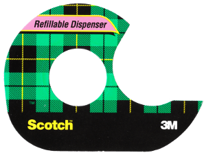
A surprising low-tech tool—Scotch Magic tape—was one of the keys to the discovery
An international group of researchers from the University of Minnesota, Argonne National Laboratory and Seoul National University have discovered a groundbreaking technique in manufacturing nanostructures that has the potential to make electrical and optical devices smaller and better than ever before. A surprising low-tech tool of Scotch Magic tape ended up being one of the keys to the discovery.
The research is published today in Nature Communications, an international online research journal.
Combining several standard nanofabrication techniques—with the final addition of the Scotch Magic tape—researchers at the University of Minnesota created extremely thin gaps through a layer of metal and patterned these tiny gaps over the entire surface of a four-inch silicon wafer. The smallest gaps were only one nanometer wide, much smaller than most researchers have been able to achieve. In addition, the widths of the gaps could be controlled on the atomic level. This work provides the basis for producing new and better nanostructures that are at the core of advanced electronic and optical devices.
One of the potential uses of nanometer-scale gaps in metal layers is to squeeze light into spaces much smaller than is otherwise possible. Collaborators at Seoul National University, led by Prof. Dai-Sik Kim, and Argonne National Laboratory, led by Dr. Matthew Pelton, showed that light could readily be squeezed through these gaps, even though the gaps are hundreds or even thousands of times smaller than the wavelength of the light used. Researchers are very interested in forcing light into small spaces because this is a way of boosting the intensity of the light. The collaborators found that the intensity inside the gaps is increased by as much as 600 million times.
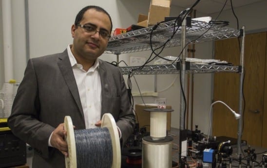
“Our technology, called atomic layer lithography, has the potential to create ultra-small sensors with increased sensitivity and also enable new and exciting experiments at the nanoscale like we’ve never been able to do before,” said Sang-Hyun Oh, one of the lead researchers on the study and a professor of electrical and computer engineering in the University of Minnesota’s College of Science and Engineering. “This research also provides the basis for future studies to improve electronic and photonic devices.”
One of the most surprising outcomes of the research is that Scotch Magic tape was one of the keys to the discovery. Etching one-nanometer-wide gaps into metals is not feasible with existing tools. Instead, the researchers in Oh’s team constructed the nano-gaps by layering atomic-scale thin films on the sides of metal patterns and then capping the structure with another metal layer. No expensive patterning tools were needed to form the gaps this way, but it was challenging to remove the excess metals on top and expose the tiny gaps. During a frustrating struggle of trying to find a way to remove the metal films, University of Minnesota Ph.D. student and lead author of the study Xiaoshu Chen found that by using simple Scotch Magic tape, the excess metals could be easily removed.
“The Scotch tape works nicely, which was unexpected,” said Oh. “Our technique is so simple yet can create uniform and ultra-small gaps like we’ve never been able to do before. We hope that it will rapidly be taken up by many researchers.”
The Latest Bing News on:
Nanofabrication
- Major Technology and Innovation Exhibitions in Germany in 2024 and 2025on April 26, 2024 at 12:30 pm
Technology and innovation exhibitions play an important role in today’s world. At no time in human history has technology changed at such an unrealistic rate. Trade shows continue to be platforms for ...
- Executive Roundtable on The Impact of U.S.-China Relations on Science & A.I. Talenton April 25, 2024 at 12:32 pm
This program is a part of our Seeking Truth Through Facts U.S.-China Program Series, which focuses on new strategic frameworks for the bilateral relationship, plurilateral relationships, rebalancing ...
- Research combines DNA origami and photolithography to move one step closer to molecular computerson April 24, 2024 at 8:49 am
Molecular computer components could represent a new IT revolution and help us create cheaper, faster, smaller, and more powerful computers. Yet researchers struggle to find ways to assemble them more ...
- Revolutionizing Nanofabrication Light-Powered 3D Printing of Helical Nanostructureson March 19, 2024 at 1:42 am
In a groundbreaking study, researchers at the University of Michigan have unveiled a revolutionary approach to nanofabrication: light-powered 3D printing of helical nanostructures. This article ...
- Top-down Nanotechnology and Its Role in Nanofabricationon February 25, 2024 at 3:58 am
Top-down nanotechnology represents a traditional approach to nanofabrication, contrasting with the atom-by-atom assembly characteristic of bottom-up methods. This technique involves starting with a ...
- Micro and Nanofabrication (MEMS)on January 22, 2023 at 6:21 am
Microfabrication and nanofabrication are the basis of manufacturing for nearly all modern miniaturized systems that are ubiquitously used in our daily life. Examples include; computer chips and ...
- Nanofabrication Labon August 17, 2020 at 9:11 pm
The Nanofabrication Lab features a state-of-the-art, 4,200 ft2 Class 100 clean room equipped with over 40 pieces of process and analytical instrumentation for complex research projects that require ...
- Core Research Facilitieson August 17, 2020 at 3:07 pm
Search our database to locate instruments and services in atomic layer deposition, material characterization, mechanical properties, nanofabrication, nuclear magnetic resonance (NMR), photo ...
- Clean Room & Nanofabrication Facilityon July 30, 2020 at 9:45 pm
The Integrated Sciences Cleanroom and Nanofabrication Facility has a 24-hour cancellation policy. Please notify the Manager at least 24 hours in advance if you can not honor your reservation. We ...
- Nanolithography and Nanofabrication Upgrade Kits: ELPHY Pluson July 24, 2019 at 1:31 am
ELPHY nanolithography and nanofabrication upgrade kits are the most ideal, versatile, and economical solution for managing the realm of Electron and Ion Beam Lithography by fast-tracking FIB-SEM, SEM, ...
The Latest Google Headlines on:
Nanofabrication
[google_news title=”” keyword=”Nanofabrication ” num_posts=”10″ blurb_length=”0″ show_thumb=”left”]
The Latest Bing News on:
Manufacturing nanostructures
- Scientists learn from caterpillars how to create self-assembling capsules for drug deliveryon April 26, 2024 at 8:00 am
Self-assembling molecules that spontaneously organize themselves to form complex structures are common in nature. For example, the tough outer layer of insects, called the cuticle, is rich in proteins ...
- Learning from caterpillars to create self-assembling capsules for drug deliveryon April 25, 2024 at 5:00 pm
Self-assembly is a cost-effective, environmentally sustainable and quick way of manufacturing nanostructures with critical applications in various industries, ranging from therapeutics to ...
- Microscope Market Navigating the Waves Future-Proofing Your Business in a Shifting Marketon April 21, 2024 at 3:56 pm
Request To Download Free Sample of This Strategic Report @- An electron microscope is a scientific imaging instrument that utilizes a beam of accelerated electrons as a source of illumination. As the ...
- Focused Ion Beam Market Overview, Size, Top Key Players, Growth, Share, and Forecast to 2024 to 2032on April 14, 2024 at 9:29 pm
Report Ocean“Focused Ion Beam Market“ report offers a comprehensive analysis of the product/service industry, spanning from 2024 to 2032. It delves into historical trends and ...
The Latest Google Headlines on:
Manufacturing nanostructures
[google_news title=”” keyword=”manufacturing nanostructures” num_posts=”10″ blurb_length=”0″ show_thumb=”left”]
