


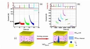
(a): Volatile (short-term) memory property of two terminal Pt/WO3-x/Pt device before the forming process. Current change observed by applying sequence of positive voltage pulses at intervals of 40 s and widths of 0.5 s. Read voltage was 0.5 V. (b): Non-volatile (long-term) memory property in the device after forming process following application of sequence of positive and negative pulses with widths of 0.1 ms. Read voltage was 0.1 V. (c): Schematic illustration of the device structures before and after forming process. (Credit: Image courtesy of International Center for Materials Nanoarchitectonics (MANA))
What's Your Reaction?
Don't Like it!
0 I Like it!
0