


Image: Chelsea Turner, MIT
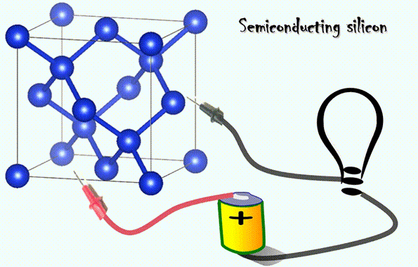
Applying just a bit of strain to a piece of semiconductor or other crystalline material can deform the orderly arrangement of atoms in its structure enough to cause dramatic changes in its properties, such as the way it conducts electricity, transmits light, or conducts heat.
Now, a team of researchers at MIT and in Russia and Singapore have found ways to use artificial intelligence to help predict and control these changes, potentially opening up new avenues of research on advanced materials for future high-tech devices.
The findings appear this week in the Proceedings of the National Academy of Sciences, in a paper authored by MIT professor of nuclear science and engineering and of materials science and engineering Ju Li, MIT Principal Research Scientist Ming Dao, and MIT graduate student Zhe Shi, with Evgeni Tsymbalov and Alexander Shapeev at the Skolkovo Institute of Science and Technology in Russia, and Subra Suresh, the Vannevar Bush Professor Emeritus and former dean of engineering at MIT and current president of Nanyang Technological University in Singapore.
Already, based on earlier work at MIT, some degree of elastic strain has been incorporated in some silicon processor chips. Even a 1 percent change in the structure can in some cases improve the speed of the device by 50 percent, by allowing electrons to move through the material faster.
Recent research by Suresh, Dao, and Yang Lu, a former MIT postdoc now at City University of Hong Kong, showed that even diamond, the strongest and hardest material found in nature, can be elastically stretched by as much as 9 percent without failure when it is in the form of nanometer-sized needles. Li and Yang similarly demonstrated that nanoscale wires of silicon can be stretched purely elastically by more than 15 percent. These discoveries have opened up new avenues to explore how devices can be fabricated with even more dramatic changes in the materials’ properties.
Strain made to order
Unlike other ways of changing a material’s properties, such as chemical doping, which produce a permanent, static change, strain engineering allows properties to be changed on the fly. “Strain is something you can turn on and off dynamically,” Li says.
But the potential of strain-engineered materials has been hampered by the daunting range of possibilities. Strain can be applied in any of six different ways (in three different dimensions, each one of which can produce strain in-and-out or sideways), and with nearly infinite gradations of degree, so the full range of possibilities is impractical to explore simply by trial and error. “It quickly grows to 100 million calculations if we want to map out the entire elastic strain space,” Li says.
That’s where this team’s novel application of machine learning methods comes to the rescue, providing a systematic way of exploring the possibilities and homing in on the appropriate amount and direction of strain to achieve a given set of properties for a particular purpose. “Now we have this very high-accuracy method” that drastically reduces the complexity of the calculations needed, Li says.
“This work is an illustration of how recent advances in seemingly distant fields such as material physics, artificial intelligence, computing, and machine learning can be brought together to advance scientific knowledge that has strong implications for industry application,” Suresh says.
The new method, the researchers say, could open up possibilities for creating materials tuned precisely for electronic, optoelectronic, and photonic devices that could find uses for communications, information processing, and energy applications.
The team studied the effects of strain on the bandgap, a key electronic property of semiconductors, in both silicon and diamond. Using their neural network algorithm, they were able to predict with high accuracy how different amounts and orientations of strain would affect the bandgap.
“Tuning” of a bandgap can be a key tool for improving the efficiency of a device, such as a silicon solar cell, by getting it to match more precisely the kind of energy source that it is designed to harness. By fine-tuning its bandgap, for example, it may be possible to make a silicon solar cell that is just as effective at capturing sunlight as its counterparts but is only one-thousandth as thick. In theory, the material “can even change from a semiconductor to a metal, and that would have many applications, if that’s doable in a mass-produced product,” Li says.
While it’s possible in some cases to induce similar changes by other means, such as putting the material in a strong electric field or chemically altering it, those changes tend to have many side effects on the material’s behavior, whereas changing the strain has fewer such side effects. For example, Li explains, an electrostatic field often interferes with the operation of the device because it affects the way electricity flows through it. Changing the strain produces no such interference.
Diamond’s potential
Diamond has great potential as a semiconductor material, though it’s still in its infancy compared to silicon technology. “It’s an extreme material, with high carrier mobility,” Li says, referring to the way negative and positive carriers of electric current move freely through diamond. Because of that, diamond could be ideal for some kinds of high-frequency electronic devices and for power electronics.
By some measures, Li says, diamond could potentially perform 100,000 times better than silicon. But it has other limitations, including the fact that nobody has yet figured out a good and scalable way to put diamond layers on a large substrate. The material is also difficult to “dope,” or introduce other atoms into, a key part of semiconductor manufacturing.
By mounting the material in a frame that can be adjusted to change the amount and orientation of the strain, Dao says, “we can have considerable flexibility” in altering its dopant behavior.
Whereas this study focused specifically on the effects of strain on the materials’ bandgap, “the method is generalizable” to other aspects, which affect not only electronic properties but also other properties such as photonic and magnetic behavior, Li says. From the 1 percent strain now being used in commercial chips, many new applications open up now that this team has shown that strains of nearly 10 percent are possible without fracturing. “When you get to more than 7 percent strain, you really change a lot in the material,” he says.
“This new method could potentially lead to the design of unprecedented material properties,” Li says. “But much further work will be needed to figure out how to impose the strain and how to scale up the process to do it on 100 million transistors on a chip [and ensure that] none of them can fail.”
“This innovative new work demonstrates potential to significantly accelerate the engineering of exotic electronic properties in ordinary materials via large elastic strains,” says Evan Reed, an associate professor of materials science and engineering at Stanford University, who was not involved in this research. “It sheds light on the opportunities and limitations that nature exhibits for such strain engineering, and it will be of interest to a broad spectrum of researchers working on important technologies.”
Learn more: Using artificial intelligence to engineer materials’ properties
The Latest on: Strain engineering
[google_news title=”” keyword=”strain engineering” num_posts=”10″ blurb_length=”0″ show_thumb=”left”]
via Google News
The Latest on: Strain engineering
- Hunter Nourzad NFL Draft 2024: Scouting Report for Kansas City Chiefs IOLon April 26, 2024 at 5:00 pm
Good grip strength, loose hips and active feet to strain, steer and finish blocks at a high level. — Potent snatch-trap technique to collapse and capitalize on overzealous, top-heavy power rushers. — ...
- UW-Madison ends alumni email accounts, citing cybersecurity risks and financial strainon April 26, 2024 at 5:35 am
"Related to email, we will now need to pay for storage for every single email account," said Mary Evansen, communications director for UW-Madison Division of Information Technology.
- Tuition hike will offload university financial pressures, may strain student budgets, expert sayson April 24, 2024 at 5:00 pm
UW–Madison’s Bursar Office notified students of a tuition increase through an email after the Board of Regents approved a 3.75% increase for all Universities of Wisconsin after a 10-year tuition ...
- strain wave gearon April 24, 2024 at 5:00 pm
[ZeroBacklash] created a little strain wave gearbox (harmonic drive) for when you want to trade speed for torque on NEMA 17 stepper motors. Strain wave gears work by deforming a stationary ...
- New monkeypox strain with sexual transmission potential raises global concernson April 24, 2024 at 7:10 am
The effectiveness of vaccines against the new variant remains unknown, although animal data shows promising results.
- Mechanical strain control of quantum transport in graphene enables new class of nanoelectronic deviceson April 23, 2024 at 5:00 pm
Platform for strain-engineering of quantum transport in 2DMs: applied theory, custom instrumentation, and device design. a) Sample holder geometry showing the bending of a Si substrate hosting a ...
- Why Don’t We Have A Cure For Cavities? Inside the Decades-Long Scientific Queston April 23, 2024 at 4:00 am
Scientists have been trying to manipulate the way our oral microbes interact with our teeth to prevent cavities for decades — they might be closer than ever.
- Riley Strain’s parents slam his frat brothers for continuing to party after he went missing: ‘Appalling’on April 17, 2024 at 10:39 am
Riley Strain’s grieving parents slammed his fraternity brothers at the University of Missouri for continuing to party after he went missing — calling their nonchalant behavior “appalling.” ...
- Riley Strain texted mom about strange-tasting drink on night he disappeared, she sayson April 17, 2024 at 6:12 am
The mother of Riley Strain — the University of Missouri student whose body was pulled from a river in Nashville — said he texted her about his drink tasting odd on the night he disappeared.
- Riley Strain texted his mother to say his drink tasted ‘strange’ shortly before he disappearedon April 16, 2024 at 5:01 pm
University of Missouri student Strain went missing shortly before 10 pm on 8 March after he was kicked out of a bar in Nashville and became separated from his friends. His body was recovered from ...
via Bing News
