


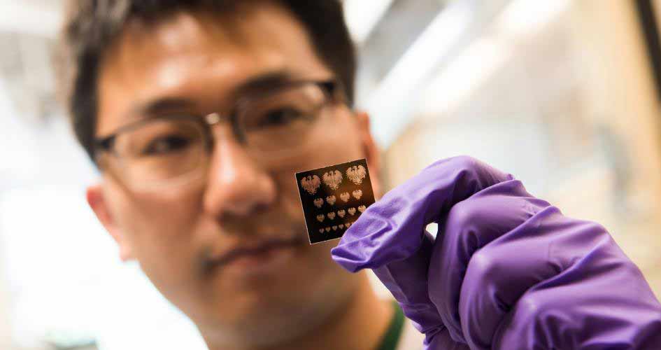
Postdoctoral researcher Yuanyuan Wang holds a ‘mask’ used in a new process that makes it easier to build nanomaterials into transistors, solar cells and other devices.
Photo byJean Lachat
UChicago, Argonne scientists create technique to build nanomaterials into electronic devices
Scientists at the University of Chicago and Argonne National Laboratory have discovered a new way to precisely pattern nanomaterials that could open a new path to the next generation of everyday electronic devices.
The new research, published in Science, is expected to make such materials easily available for eventual use in everything from LED displays to cellular phones to photodetectors and solar cells. Though nanomaterials are promising for future devices, ways to build them into complex structures have been limited and small-scale.
“This is a step needed to move quantum dots and many other nanomaterials from proof-of-concept experiments to real technology we can use,” said co-author Dmitri Talapin, professor of chemistry at UChicago and a scientist with the Center for Nanoscale Materials at Argonne. “It really expands our horizons.”

Courtesy ofDmitri Talapin and Yuanyuan Wang / Illustration by UChicago Creative
But the method has its limitations. Only a few materials can be patterned this way; it was originally developed for silicon, and as silicon’s half-century reign over electronics reaches its end, scientists are looking ahead to the next materials.
One such avenue of interest is nanomaterials—tiny crystals of metals or semiconductors. At this scale, they can have unique and useful properties, but manufacturing devices out of them has been difficult.
The new technique, called DOLFIN, makes different nanomaterials directly into “ink” in a process that bypasses the need to lay down a polymer stencil. Talapin and his team carefully designed chemical coatings for individual particles. These coatings react with light, so if you shine light through a patterned mask, the light will transfer the pattern directly into the layer of nanoparticles below—wiring them into useful devices.
“We found the quality of the patterns was comparable to those made with state-of-the-art techniques,” said lead author Yuanyuan Wang, postdoctoral researcher at UChicago. “It can be used with a wide range of materials, including semiconductors, metals, oxides or magnetic materials—all commonly used in electronics manufacturing.”

Learn more: New method promises easier nanoscale manufacturing
The Latest on: Nanoscale manufacturing
[google_news title=”” keyword=”nanoscale manufacturing” num_posts=”10″ blurb_length=”0″ show_thumb=”left”]- Mitsubishi, Denka Collaborate for Fullerene Businesson May 2, 2024 at 12:24 am
Under a joint venture agreement between Denka and Mitsubishi Corporation, Denka will acquire from Mitsubishi a 50 % stake in Frontier Carbon Corporation, a company dedicated to the manufacturing and ...
- Patitz Awarded NSF Grant for Research on DNA-Based Nanostructure Researchon May 1, 2024 at 10:15 pm
Matthew Patitz, associate professor, plans to construct nanoscale structures using DNA sequences designed to fold into elongated slats that then form complex geometries.
- Cleveland Manufacturing Newson April 29, 2024 at 8:48 am
The Business Journals' Book of Lists provides you with more than 1,000 of the hottest area companies in their fields, by ranking. Showcase your company news with guaranteed exposure both in print ...
- Dayton Manufacturing Newson April 29, 2024 at 2:38 am
Excel Title Services, a leading provider of comprehensive title solutions, is pleased to announce its… INDIANAPOLIS, INDIANA — Hays + Sons is thrilled to announce the opening of its newest ...
- The Realities Of AI In Manufacturingon April 17, 2024 at 3:30 am
According to the World Economic Forum, the global manufacturing AI market was worth over $3 billion in 2023 and is expected to increase to over $20 billion by 2028. The use cases grow each day ...
- New iPhone 16 Camera Treatment May Put an End to Lens Flareon April 15, 2024 at 3:01 pm
According to the latest iPhone 16 Pro supply chain rumor, Apple has been testing new anti-reflective optical coating technologies for its iPhone cameras to help eliminate lens flares and artifacts ...
- An Intelligent Future for Manufacturingon April 11, 2024 at 5:00 pm
Digitalisation plays a key role in the evolution of manufacturing industries. Foundry’s Digital Business Study 2023 shows that 93% of manufacturers surveyed have adopted or plan to adopt a ...
- A molecular moon lander: Insight into molecular motion on surfaces at the nanoscaleon April 11, 2024 at 11:46 am
The process is critical to numerous applications, including catalysis and the manufacturing of nanoscale devices. Now, using neutron spectroscopy experiments performed at Institut Laue-Langevin ...
- A molecular moon lander: Insight into molecular motion on surfaces at the nanoscaleon April 10, 2024 at 5:00 pm
The process is critical to numerous applications, including catalysis and the manufacturing of nanoscale devices. The work is published in the journal Communications Chemistry. In fact ...
- Meet the ‘quantum plumbers’ uncovering the mysteries of fluid mechanics at the nanoscaleon April 8, 2024 at 5:00 pm
Nanofluidics could be used to purify water, generate energy and build nanoscale machines. But when water flows through a carbon nanotube, classical fluid mechanics breaks down, leading to puzzling ...
via Google News and Bing News
