“This is a quite remarkable spatial resolution.”
Researchers have created tiny holograms using a “metasurface” capable of the ultra-efficient control of light, representing a potential new technology for advanced sensors, high-resolution displays and information processing.
The metasurface, thousands of V-shaped nanoantennas formed into an ultrathin gold foil, could make possible “planar photonics” devices and optical switches small enough to be integrated into computer chips for information processing, sensing and telecommunications, said Alexander Kildishev, associate research professor of electrical and computer engineering at Purdue University.
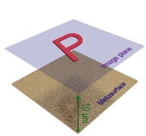
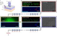
Laser light shines through the nanoantennas, creating the hologram 10 microns above the metasurface. To demonstrate the technology, researchers created a hologram of the word PURDUE smaller than 100 microns wide, or roughly the width of a human hair.
“If we can shape characters, we can shape different types of light beams for sensing or recording, or, for example, pixels for 3-D displays. Another potential application is the transmission and processing of data inside chips for information technology,” Kildishev said. “The smallest features – the strokes of the letters – displayed in our experiment are only 1 micron wide. This is a quite remarkable spatial resolution.”
Findings are detailed in a research paper appearing on Friday (Nov. 15) in the journal Nature Communications.
Metasurfaces could make it possible to use single photons – the particles that make up light – for switching and routing in future computers. While using photons would dramatically speed up computers and telecommunications, conventional photonic devices cannot be miniaturized because the wavelength of light is too large to fit in tiny components needed for integrated circuits.
Nanostructured metamaterials, however, are making it possible to reduce the wavelength of light, allowing the creation of new types of nanophotonic devices, said Vladimir M. Shalaev, scientific director of nanophotonics at Purdue’s Birck Nanotechnology Center and a distinguished professor of electrical and computer engineering.
“The most important thing is that we can do this with a very thin layer, only 30 nanometers, and this is unprecedented,” Shalaev said. “This means you can start to embed it in electronics, to marry it with electronics.”
Go deeper with Bing News on:
Hologram technology
- Swave Photonics develops true holographic display for spatial computing
Swave Photonics, a "true holographic display" company, announced the world’s first 3D holographic display technology for XR.
- Swave Photonics debuts Holographic eXtended Reality display with tiny-pixel technology
Holographic display startup Swave Photonics today announced the development of what is claimed to be the world’s first 3D holographic display technology for compact extended reality form factors such ...
- Swave Photonics Developing World’s First True Holographic Display Technology To Power Reality-First Spatial Computing
Emerging category of display technology delivers world’s smallest pixel to steer light, render vivid 3D images LEUVEN, Belgium & SILICON VALLEY, Calif., April 25, 2024--(BUSINESS WIRE)--Swave ...
- Holographic displays offer a glimpse into an immersive future
Setting the stage for a new era of immersive displays, researchers are one step closer to mixing the real and virtual worlds in an ordinary pair of eyeglasses using high-definition 3D holographic ...
- WiMi Hologram Cloud Announced the B-TEC Technology to Enhance Information Security
WiMi Hologram Cloud Inc. (NASDAQ: WIMI) ("WiMi" or the "Company"), a leading global Hologram Augmented Reality ("AR") Technology provider, today announced that it developed an embedded steganographic ...
Go deeper with Google Headlines on:
Hologram technology
[google_news title=”” keyword=”Hologram technology” num_posts=”5″ blurb_length=”0″ show_thumb=”left”]
Go deeper with Bing News on:
Holograms
- Demand for Apple's HoloLens-like Vision Pro has fallen 'well beyond' expectations. I am shocked. Not really.
Remember the Apple Vision Pro hype from a few months ago? Me neither. Seems nobody else does either, since according to a new report, nobody actually wants to wear a $3000 computer on their face.
- ARHT Holograms Enhances AtkinsRéalis' Booth Experience at Passenger Terminal Expo 2024 in Germany
ARHT was founded in 2014 and is publicly traded on the TSX Venture Exchange. ARHT has offices in North America, Europe and Asia and operates from its own studios in locations from Toronto to Singapore ...
- Revolutionizing 3D: New Holographic Technique Breaks Computational Barriers
A groundbreaking approach utilizes a split Lohmann lens-based diffraction model for the real-time creation of Computer-Generated Holography (CGH), dramatically lowering computational demands while ...
- ARHT Holograms Enhances AtkinsRéalis' Booth Experience at Passenger Terminal Expo 2024 in Germany
TORONTO, April 16, 2024 (GLOBE NEWSWIRE) -- ARHT Media Inc. ("ARHT" or "the Company") (TSXV: ART), (OTCQB: ARHTF) the global leader in the development, production and distribution of high-quality ...
- Celebrity-Backed Proto Puts Holograms in a Four Seasons Hotel
Guests at the Beverly Wilshire hotel can now interact with holographic versions of staff projected into their rooms.
Go deeper with Google Headlines on:
Holograms
[google_news title=”” keyword=”holograms” num_posts=”5″ blurb_length=”0″ show_thumb=”left”]

