


He is developing next-generation, nanoscale transistors for integrated electronics
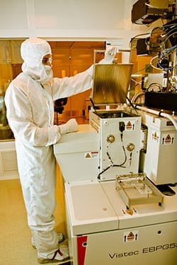
The new electron beam writer housed in the Nano3 cleanroom facility at the Qualcomm Institute is important for electrical engineering professor Shadi Dayeh’s two major areas of research. He is developing next-generation, nanoscale transistors for integrated electronics; and he is developing neural probes that have the capacity to extract electrical signals from individual brain cells and transmit the information to a prosthetic device or computer. Achieving this level of signal extraction or manipulation requires tiny sensors spaced very closely together for the highest resolution and signal acquisition. Enter the new electron beam writer.
Electron beam (e-beam) lithography enables researchers to write very small patterns on large substrates with a high level of precision. It is a widely used tool in information technology and life science. Applications range from writing patterns on silicon and compound semiconductor chips for electronic device and materials research to genome sequencing platforms. But the ability to write patterns on the scale afforded by the Nano3 facility—with its minimum feature size of less than 8 nanometers on wafers with diameters that can be as large as 8 inches—is unique in Southern California. Before the facility opened earlier this year, the closest comparable e-beam writer was in Los Angeles. In an e-beam writer, unique patterns are “written” on a silicon wafer coated with a polymer resist layer that is sensitive to electron irradiation. The machine directs a narrowly focused electron beam onto the surface marking the pattern, making parts of the resist coating insoluble and others soluble. The soluble area is later washed away, revealing the pattern which can have sub-10 nanometer feature dimensions.
Bioengineering professor Todd Coleman will use the new e-beam writer as one essential step in the building of his epidermal, or tattoo, electronic devices. The devices are designed to acquire brain signals for a variety of medical applications, from monitoring infants for seizures in neonatal intensive care to studying the cognitive impairment associated with Alzheimer’s disease or dementia, and soldiers struggling with post-traumatic stress syndrome.
Electrical engineering Ph.D. candidate Andrew Grieco is using the machine to develop a new type of optical waveguide that promises to improve efficiency and reduce power consumption. Grieco works in the laboratory of Shaya Fainman, professor and chair, Department of Electrical and Computer Engineering. Developing on-chip optical networking devices such as waveguides, switches and amplifiers is a critical step in the development of optical chips. Although information systems rely primarily on fiber-optic networks to connect and share data around the world, the underlying computer technology is still based on electronic chips, causing data traffic jams.
The Latest Bing News on:
Electron Beam Writer
- Electron Beam Induced Deposition (EBID): Nanoscale 3D Printing with Electronson April 13, 2024 at 1:40 am
It is essentially a form of 3D printing at the nanoscale, where the electron beam acts as a "pen" to directly write three-dimensional nanostructures. Schematic illustration of the EBID process. A ...
- Dielectric laser accelerator creates focused electron beamon April 10, 2024 at 8:57 am
How it could work: electrons are injected into the dielectric laser accelerator (centre) from a source at the top left. The cavities are within the turquoise and gold bars, which are illuminated with ...
- E-Beam Lithography System (100kV) – Elionix ELS-G100on March 26, 2024 at 5:00 pm
The Elionix ELS-G100 electron beam lithography system produces a highly stable beam with a diameter as small 1.8nm, using acceleration voltages of up to 100kV and high beam currents. This allows fine ...
- Development of Electron Beam and X Ray Applications for Food Irradiationon December 18, 2023 at 12:25 am
including high energy (MeV) and low energy (keV) electron beam and X ray irradiation. Comparative studies of gamma, electron beam and X ray irradiation for food and phytosanitary uses are also ...
- The Different Types of Lithography in Nanotechnologyon June 16, 2023 at 11:43 am
On the other hand, Electron Beam, Focused Ion Beam, and Dip Pen Nanolithography are slower, serial processes. They require the beam or tip to be scanned across the surface to write each feature, ...
- How nuclear physicists at Jefferson Lab found something ‘strange’ in the ordinaryon April 25, 2023 at 4:46 am
When a high-energy electron from the beam reached one of these targets ... Kandice Carter, external communications and science writer for the lab, said the next experiment that will take data ...
- Vistec SB254: High Performance Electron-Beam Lithographyon December 22, 2022 at 11:24 am
Based on the Variable Shaped Beam (VSB) principle, these tools are utilized in a wide range of existing and emerging semiconductor and nanotechnology applications including silicon direct write, ...
- electron-beam lithographyon December 4, 2022 at 4:00 pm
He shares the results of his electron-beam lithography experiments in his latest video (embedded below). In e-beam lithography, or EBL, shapes are drawn onto a wafer using an electron beam in a ...
- VOYAGER: The electron beam lithography system for results at the push of a buttonon August 17, 2020 at 4:18 pm
The VOYAGER is a high-performance electron beam lithography system that has been specifically ... Depending on the pattern, writing speeds of more than 1 cm²/hour could be obtained at the highest ...
- eLINE Plus: Ultra High Resolution Electron Beam Lithography, Nanoengineering and Imagingon July 10, 2017 at 4:11 am
The smallest electron beam size of 1.6 nm, delivered by an EBL system ... losing time or compromising the entire benefit of either nanofabrication method. Write with two hands simultaneously and make ...
The Latest Google Headlines on:
Electron Beam Writer
[google_news title=”” keyword=”Electron Beam Writer” num_posts=”10″ blurb_length=”0″ show_thumb=”left”]
The Latest Bing News on:
Nanoscale transistors
- Mechanical strain control of quantum transport in graphene enables new class of nanoelectronic deviceson April 23, 2024 at 5:00 pm
Possibilities include mechanically gated transistors, strain-tunable qubits ... One limitation is that the strain fields are still not completely uniform at the nanoscale. Integrating strain control ...
- Atom-by-atom: Imaging structural transformations in 2D materialson April 18, 2024 at 5:56 pm
Silicon-based electronics are approaching their physical limitations and new materials are needed to keep up with current technological demands. Two-dimensional (2D) materials have a rich array of ...
- Graphene’s Light-Speed Electrons Promise Revolution in Nanoscale Transistorson April 18, 2024 at 3:24 pm
Researchers have shown that double-layer graphene can function both as a superconductor and an insulator, a property that could revolutionize transistor technology. This dual functionality allows for ...
- Single-Molecule Transistor Using Quantum Interferenceon April 16, 2024 at 2:35 pm
A new technical paper titled “Quantum interference enhances the performance of single-molecule transistors” was published by researchers at Queen Mary University of London, University of Oxford, ...
- Quantum electronics: Charge travels like light in bilayer grapheneon April 16, 2024 at 11:13 am
An international research team has demonstrated experimentally that electrons in naturally occurring double-layer graphene move like particles without any mass, in the same way that light travels.
- International Research Team Demonstrates Potential for Nanoscale Transistors in All-Carbon Filmon April 16, 2024 at 9:08 am
An international research team led by the University of Göttingen has demonstrated experimentally that electrons in naturally occurring double-layer graphene move like particles without any mass, in ...
- Nanoscale devices articles from across Nature Portfolioon March 31, 2024 at 5:00 pm
Examples of nanoscale devices are synthetic molecular motors such as rotaxanes, graphene-based transistors and nanoelectromechanical oscillators. How can light be efficiently manipulated below the ...
- Quantum interference could lead to smaller, faster, and more energy-efficient transistorson March 25, 2024 at 10:55 am
Transistors are the basic building blocks ... that can be used with different materials to remove this effect. In the nanoscale structures that Professor Jan Mol, Dr. James Thomas, and their ...
- Nanofluidic Transistors: Controlling Fluids at the Nanoscaleon March 14, 2024 at 3:50 am
Nanofluidic transistors, also known as nanofluidic systems or nanofluidic devices, are innovative tools that control the flow of fluids, such as water or ions, through nanoscale channels using ...
- Selective operation of enhancement and depletion modes of nanoscale field-effect transistorson March 6, 2024 at 1:52 pm
More information: Abhay A. Sagade, Selective Operation of Enhancement and Depletion Modes of Nanoscale Field-Effect Transistors, ACS Applied Electronic Materials (2024). DOI: 10.1021/acsaelm.3c01825 ...
The Latest Google Headlines on:
Nanoscale transistors
[google_news title=”” keyword=”nanoscale transistors” num_posts=”10″ blurb_length=”0″ show_thumb=”left”]

