


Credit: Marti/JILA
In the nanoworld, tiny particles of gold can operate like snow blowers, churning through surface layers of an important class of semiconductors to dig unerringly straight paths. The surprising trenching capability, reported by scientists from the National Institute of Standards and Technology (NIST) and IBM,* is an important addition to the toolkit of nature-supplied “self-assembly” methods that researchers aim to harness for making useful devices.
Foreseeable applications include integrating lasers, sensors, wave guides and other optical components into so-called lab-on-a-chip devices now used for disease diagnosis, screening experimental materials and drugs, DNA forensics and more. Easy to control, the new gold-catalyzed process for creating patterns of channels with nanoscale dimensions could help to spawn entirely new technologies fashioned from ensembles of ultra-small structures.
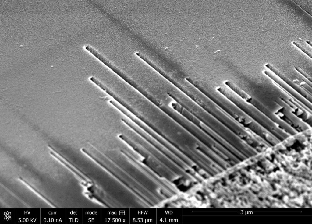
Preliminary research results that began as lemons—a contaminant-caused failure that impeded the expected formation of nanowires—eventually turned into lemonade when scanning electron microscope images revealed long, straight channels.
“We were disappointed, at first,” says NIST research chemist Babak Nikoobakht. “Then we figured out that water was the contaminant in the process—a problem that turned out to be a good thing.”
That’s because, as determined in subsequent experiments, the addition of water vapor served to transform gold nanoparticles into channel diggers, rather than the expected wire makers. Beginning with studies on the semiconductor indium phosphide, the team teased out the chemical mechanisms and necessary conditions underpinning the surface-etching process.
First, they patterned the surface of the semiconductor by selectively coating it with a gold layer only a few nanometers thick. Upon heating, the film breaks up into tiny particles that become droplets. The underlying indium phosphide dissolves into the gold nanoparticles above, creating a gold alloy. Then, heated water vapor is introduced into the system. At temperatures below 300 degrees Celsius (572 degrees Fahrenheit), the tiny gold-alloy particles, now swathed with water molecules, etch nanoscale pits into the indium phosphide.
But at 440 degrees Celsius (824 degrees Fahrenheit) and above, long V-shaped nanochannels formed. The channels followed straight paths dictated by the regularly repeating lattice of atoms in the crystalline semiconductor. During the process, indium and phosphorous atoms interact with oxygen atoms in the water molecules on the surface of the gold alloy droplet. The oxidized indium and phosphorous evaporate, and the droplet advances, picking up more semiconductor atoms to oxidize as it goes.
In effect, the droplet is the chemical equivalent of the auger on a snow blower that, instead of snow, burrows through the top portion of the semiconductor and ejects evaporated bits, Nikoobakht explains.
The team observed the same phenomena in gallium phosphide and indium arsenide, two more examples of semiconductors formed by combining elements from the third and fifth columns of the periodic table. Compound semiconductors in this class are used to make LEDs, and for communications, high-speed electronics and many other applications. Nikoobakht believes that, with adjustments, the etching process might also work for creating patterns of channels on silicon and other materials.
Controllable, fast and flexible, the “bottom up” channel-fabrication process shows promise for use on industrial scales, the researchers suggest. In their article, the teams describe how they used the process to etch patterns of hollow channels like those used to direct the flow of liquids, such as a blood sample, in a microfluidic device, or lab on a chip.
Read more: Nanoworld “Snow Blowers” Carve Straight Channels in Semiconductor Surfaces
The Latest on: Channel-fabrication process
[google_news title=”” keyword=”channel-fabrication process” num_posts=”10″ blurb_length=”0″ show_thumb=”left”]
via Google News
The Latest on: Channel-fabrication process
- Mitsubishi Electric India Unveils all new Cutting-Edge M80LA CNC for Turning Segmenton April 30, 2024 at 6:29 am
Mitsubishi Electric India offers advanced CNC control systems to take the machining needs of customers to a higher performance level. The company supplies CNC package and technologies to various ...
- Industrial IoT: Transforming Manufacturing Processeson April 29, 2024 at 8:21 pm
The rise of emerging technologies and Internet of Things (IoT) applications in industrial systems is facilitating the development of Industrial IoT (IIoT). In the industrial sector, IIoT serves as a ...
- Aussiebum plans to set up manufacturing facility in Indiaon April 26, 2024 at 2:10 am
Australian brand AussieBum plans to establish a manufacturing unit in India to produce men's swimwear, underwear, and clothing for domestic and global markets. With aims to capture 3-5% of India's ...
- Apple's go-to chipmaker TSMC unveils 1.6nm process for 2026 chips: Detailson April 25, 2024 at 11:20 pm
While the 1.6nm process is slated for 2026 chips, TSMC is set to kick off the production of the 2nm architecture process for debut in 2025 with Apple iPhones ...
- ICEA bats for chip design, manufacturing to be treated as strategic sectoron April 25, 2024 at 10:45 am
Industry body ICEA has recommended various measures, including encouraging large Indian corporates to invest in semiconductor design and treating chip design and manufacturing as a strategic sector, ...
- TSMC unveils A16 manufacturing process for 1.6nm chips in challenge to Intel's claimson April 25, 2024 at 4:56 am
A16, set to enter production in the second half of 2026, will use leading nanosheet transistors and what TSMC calls an "innovative" backside power rail solution ...
- More foreign companies moving manufacturing facilities from China to Malaysia amid trade tensionson April 22, 2024 at 10:33 am
Semiconductor and electric vehicle companies have been relocating to Southeast Asia to bypass trade restrictions between China and the United States, as well as strengthen their supply chains.
- Predicting And Preventing Process Drifton April 21, 2024 at 5:00 pm
Drift can occur in any of the hundreds of process steps involved in manufacturing a single wafer, subtly altering the electrical properties of chips and leading to functional and reliability issues.
- Boeing and the Dark Age of American Manufacturingon April 19, 2024 at 4:59 pm
would instead appear as overhead—creating the impression that in-house work was expensive and furthering the rationale for offloading even more of the manufacturing process. In the short term ...
- Energy Considerations at the Dawn of Strategic Manufacturingon April 18, 2024 at 5:00 pm
A new era of U.S. industrial policy has begun thanks to three pieces of recent federal legislation: the Infrastructure Investment and Jobs Act (IJJA), the CHIPS and Science Act (CHIPS act), and the ...
via Bing News
