Transistors based on carbon nanostructures: what sounds like a futuristic dream could be reality in just a few years’ time. An international research team working with Empa has now succeeded in producing nanotransistors from graphene ribbons that are only a few atoms wide, as reported in the current issue of “Nature Communications”.
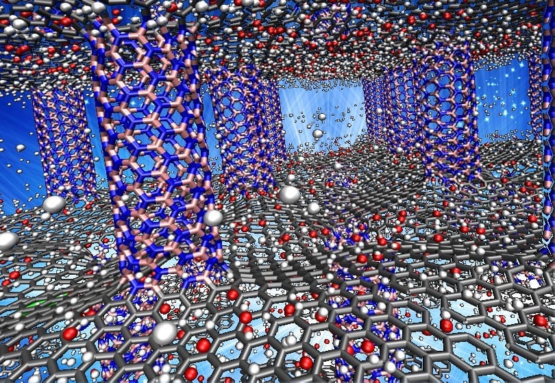
Graphene ribbons that are only a few atoms wide, so-called graphene nanoribbons, have special electrical properties that make them promising candidates for the nanoelectronics of the future: while graphene – a one atom thin, honeycomb-shaped carbon layer – is a conductive material, it can become a semiconductor in the form of nanoribbons. This means that it has a sufficiently large energy or band gap in which no electron states can exist: it can be turned on and off – and thus may become a key component of nanotransistors.
The smallest details in the atomic structure of these graphene bands, however, have massive effects on the size of the energy gap and thus on how well-suited nanoribbons are as components of transistors. On the one hand, the gap depends on the width of the graphene ribbons, while on the other hand it depends on the structure of the edges. Since graphene consists of equilateral carbon hexagons, the border may have a zigzag or a so-called armchair shape, depending on the orientation of the ribbons. While bands with a zigzag edge behave like metals, i.e. they are conductive, they become semiconductors with the armchair edge.
This poses a major challenge for the production of nanoribbons: if the ribbons are cut from a layer of graphene or made by cutting carbon nanotubes, the edges may be irregular and thus the graphene ribbons may not exhibit the desired electrical properties.
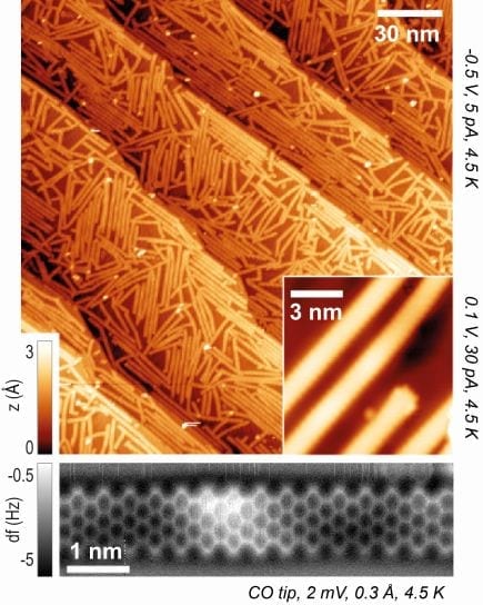
Empa researchers in collaboration with the Max Planck Institute for Polymer Research in Mainz and the University of California at Berkeley have now succeeded in growing ribbons exactly nine atoms wide with a regular armchair edge from precursor molecules. The specially prepared molecules are evaporated in an ultra-high vacuum for this purpose. After several process steps, they are combined like puzzle pieces on a gold base to form the desired nanoribbons of about one nanometer in width and up to 50 nanometers in length.
These structures, which can only be seen with a scanning tunneling microscope, now have a relatively large and, above all, precisely defined energy gap. This enabled the researchers to go one step further and integrate the graphene ribbons into nanotransistors. Initially, however, the first attempts were not very successful: Measurements showed that the difference in the current flow between the “ON” state (i.e. with applied voltage) and the “OFF” state (without applied voltage) was far too small. The problem was the dielectric layer of silicon oxide, which connects the semiconducting layers to the electrical switch contact. In order to have the desired properties, it needed to be 50 nanometers thick, which in turn influenced the behavior of the electrons.
However, the researchers subsequently succeeded in massively reducing this layer by using hafnium oxide(HfO2) instead of silicon oxide as the dielectric material. The layer is therefore now only 1.5 nanometers thin and the “on”-current is orders of magnitudes higher.
Another problem was the incorporation of graphene ribbons into the transistor. In the future, the ribbons should no longer be located criss-cross on the transistor substrate, but rather aligned exactly along the transistor channel. This would significantly reduce the currently high level of non-functioning nanotransistors.
Learn more: A nanotransistor made of graphene
The Latest on: Graphene nanotransistor
[google_news title=”” keyword=”graphene nanotransistor” num_posts=”10″ blurb_length=”0″ show_thumb=”left”]- Graphene in Biomedicine: Opportunities and Challengeson April 27, 2024 at 5:00 pm
Graphene, whose discovery won the 2010 Nobel Prize in physics, has been a shining star in the material science in the past few years. Owing to its interesting electrical, optical, mechanical and ...
- Local twist angles in graphene come into viewon April 18, 2024 at 5:00 pm
The new technique revealed pronounced variations in local twist angles in twisted bilayer graphene. (Courtesy: S Zhu) Stacking layers of two-dimensional materials on top of each other and varying the ...
- Goldene: New 2D form of gold makes graphene look boringon April 17, 2024 at 12:29 am
Graphene is a bit like the Novak Djokovic of materials – it’s so damn talented that each new achievement feels passé. But now, an exciting new upstart is challenging graphene’s title.
- Unlocking exotic physics: Exploring graphene's topological bands in super-moiré structureson April 3, 2024 at 5:00 pm
Graphene is a 2D sheet of carbon atoms arranged in a hexagonal lattice (arrangement) which demonstrates properties like high electrical conductivity, mechanical strength, and flexibility. This has ...
- Electrons become fractions of themselves in graphene, study findson February 21, 2024 at 8:16 am
Now, MIT physicists have observed the elusive fractional charge effect, this time in a simpler material: five layers of graphene—an atom-thin layer of carbon that stems from graphite and common ...
- ‘Wonder material’ graphene makes huge step towards practical useon February 16, 2024 at 2:19 am
Graphene, a “wonder material” that could help solve some of humanity’s deepest problems, has cleared a major hurdle towards practical uses. Graphene is the world’s thinnest, super-strong ...
- Breakthroughs in graphene synthesison May 7, 2023 at 1:36 am
Scientists in Brazil have made the largest chemically synthesised graphene sheet ever reported. Graphene – single-atom-thick sheets of carbon – is a material that has seemed full of possibilities ...
- Is Graphene Green?on December 25, 2022 at 4:08 pm
As assessed in IDTechEx's latest report, "Graphene Market & 2D Materials Assessment 2023-2033", the capacity for graphene easily exceeds 12,000 tpa. Nearly all of this comes from a graphite feedstock ...
- Graphene Oxide In Pfizer Covid-19 Vaccines? Here Are The Latest Unsupported Claimson July 10, 2021 at 1:54 pm
One example of such a claim was an Instagram post that stated: “99% Graphene Oxide in Pfizer V4X? Spanish scientists obtain vial of Pfizer v4xin3 and find that 98-99%.” In this case ...
- 3D Grapheneon August 13, 2020 at 6:15 pm
3D graphene refers to a material that consists of a graphene-based framework that has a porous, three-dimensional structure. This material can be referred to as a graphene aerogel or a 3D-printed ...
via Google News and Bing News

