


Dozens of new two-dimensional materials similar to graphene are now available, thanks to research from University of Manchester scientists.
These 2D crystals are capable of delivering designer materials with revolutionary new properties.
The problem has been that the vast majority of these atomically thin 2D crystals are unstable in air, so react and decompose before their properties can be determined and their potential applications investigated.
Writing in NanoLetters, the University of Manchester team demonstrate how tailored fabrication methods can make these previously inaccessible materials useful.
By protecting the new reactive crystals with more stable 2D materials, such as graphene, via computer control in a specially designed inert gas chamber environments, these materials can be successfully isolated to a single atomic layer for the first time.
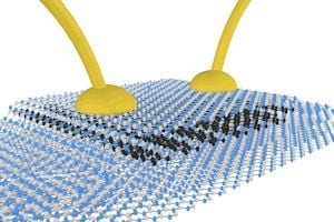
Combining a range of 2D materials in thin stacks give scientists the opportunity to control the properties of the materials, which can allow ‘materials-to-order’ to meet the demands of industry.
High-frequency electronics for satellite communications, and light weight batteries for mobile energy storage are just two of the application areas that could benefit from this research. The breakthrough could allow for many more atomically thin materials to be studied separately as well as serve as building blocks for multilayer devices with such tailored properties.
The team, led by Dr Roman Gorbachev, used their unique fabrication method on two particular two-dimensional crystals that have generated intense scientific interest in the past 12 months but are unstable in air: black phosphorus and niobium diselenide.
The technique the team have pioneered allows the unique characteristics and excellent electronic properties of these air-sensitive 2D crystals to be revealed for the first time.
The isolation of graphene in 2004 by a University of Manchester team lead by Sir Andre Geim and Sir Kostya Novoselov led to the discovery of a range of 2D materials, each with specific properties and qualities.
Dr Gorbachev said: “This is an important breakthrough in the area of 2D materials research, as it allows us to dramatically increase the variety of materials that we can experiment with using our expanding 2D crystal toolbox.
“The more materials we have to play with, the greater potential there is for creating applications that could revolutionise the way we live.” Sir Andre Geim added.
Read more: Manchester team reveal new, stable 2D materials

The Latest on: 2D materials
[google_news title=”” keyword=”2D materials” num_posts=”10″ blurb_length=”0″ show_thumb=”left”]
via Google News
The Latest on: 2D materials
- 2D all-organic perovskites: potential use in 2D electronicson May 9, 2024 at 12:09 pm
Perovskites are among the most researched topics in materials science. Recently, a research team has solved an age-old challenge to synthesize all-organic two-dimensional perovskites, extending the ...
- PolyU researchers create 2D all-organic perovskites and demonstrate potential use in 2D electronicson May 9, 2024 at 7:04 am
Prof. Loh Kian Ping, Chair Professor of Materials Physics and Chemistry and Global STEM Professor of the Department of Applied Physics of PolyU, led a team in the successful synthesis and device ...
- Researchers 'unzip' 2D materials with laserson May 7, 2024 at 8:42 am
In a new paper published on May 1 in the journal Science Advances, researchers at Columbia Engineering used commercially available tabletop lasers to create tiny, atomically sharp nanostructures, or ...
- Researchers esearchers 'unzip' 2D materials with laserson May 6, 2024 at 4:59 pm
To explore what they could do with their nanopatterned samples, the engineering team teamed up with physicist Dmitri Basov’s lab, which specializes in creating and controlling nano-optical effects in ...
- Columbia researchers “unzip” 2D materials with laserson May 6, 2024 at 4:59 pm
In a new paper in the journal Science Advances, researchers used commercially available tabletop lasers to create tiny, atomically sharp nanostructures in samples of a layered 2D material called ...
- New high-throughput device to unlock the potential of advanced materialson May 6, 2024 at 12:33 pm
A Birmingham researcher has developed a new high-throughput device that produces libraries of nanomaterials using sustainable mechanochemical approaches.
- Researchers create 2D all-organic perovskites, demonstrate potential use in 2D electronicson May 6, 2024 at 6:49 am
Perovskites are among the most researched topics in materials science. Recently, a research team from The Hong Kong Polytechnic University (PolyU) has solved an age-old challenge to synthesize ...
- Revolutionizing Photonics: 2D Materials Manipulate Light With Remarkable Precisionon May 4, 2024 at 3:37 pm
NYU Abu Dhabi researchers have unveiled a novel 2D material improving optical modulation for advanced systems and communications. Responding to the increasing demand for efficient, tunable optical mat ...
- Design strategies toward plasmon-enhanced 2D material photodetectorson April 29, 2024 at 1:28 pm
Traditional semiconductors such as Si, GaAs, and HgCdTe seem unable to meet the development trend of electronic devices that feature ultra-small volume, lightweight, and low power consumption. These ...
- Beyond Graphene: A New World of 2D Materials Is Opening Upon April 28, 2024 at 9:07 pm
Materials that are incredibly thin, only a few atoms thick, exhibit unique properties that make them appealing for energy storage, catalysis, and water purification. Researchers at Linköping ...
via Bing News

