


“This is a quite remarkable spatial resolution.”
Researchers have created tiny holograms using a “metasurface” capable of the ultra-efficient control of light, representing a potential new technology for advanced sensors, high-resolution displays and information processing.
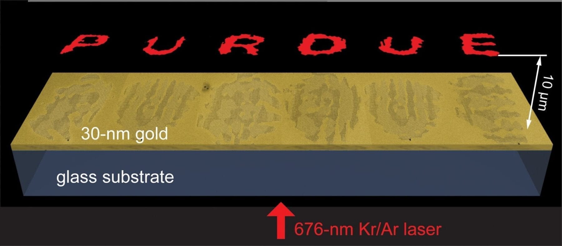
The metasurface, thousands of V-shaped nanoantennas formed into an ultrathin gold foil, could make possible “planar photonics” devices and optical switches small enough to be integrated into computer chips for information processing, sensing and telecommunications, said Alexander Kildishev, associate research professor of electrical and computer engineering at Purdue University.
Laser light shines through the nanoantennas, creating the hologram 10 microns above the metasurface. To demonstrate the technology, researchers created a hologram of the word PURDUE smaller than 100 microns wide, or roughly the width of a human hair.
“If we can shape characters, we can shape different types of light beams for sensing or recording, or, for example, pixels for 3-D displays. Another potential application is the transmission and processing of data inside chips for information technology,” Kildishev said. “The smallest features – the strokes of the letters – displayed in our experiment are only 1 micron wide. This is a quite remarkable spatial resolution.”
Findings are detailed in a research paper appearing on Friday (Nov. 15) in the journal Nature Communications.
Metasurfaces could make it possible to use single photons – the particles that make up light – for switching and routing in future computers. While using photons would dramatically speed up computers and telecommunications, conventional photonic devices cannot be miniaturized because the wavelength of light is too large to fit in tiny components needed for integrated circuits.
Nanostructured metamaterials, however, are making it possible to reduce the wavelength of light, allowing the creation of new types of nanophotonic devices, said Vladimir M. Shalaev, scientific director of nanophotonics at Purdue’s Birck Nanotechnology Center and a distinguished professor of electrical and computer engineering.
“The most important thing is that we can do this with a very thin layer, only 30 nanometers, and this is unprecedented,” Shalaev said. “This means you can start to embed it in electronics, to marry it with electronics.”
The Latest Google Headlines on:
Holograms
[google_news title=”” keyword=”Holograms” num_posts=”10″ blurb_length=”0″ show_thumb=”left”]
The Latest Bing News on:
Holograms
- SBJ Tech: Bears use 3D holograms to intro NFL Draft picks to fanson May 1, 2024 at 2:47 pm
As Caleb Williams spoke to Bears fans during the team’s NFL Draft party at Soldier Field, one of the first questions to him focused on checking off a big box on the career milestone list -- becoming ...
- Bears tap Proto Epic tech to beam in top picks Caleb Williams, Rome Odunzeon May 1, 2024 at 2:42 pm
Bears QB Caleb Williams, along with the Bears’ other first-round pick, Rome Odunze, appeared at Soldier Field on Draft Day as three-dimensional holograms via a Proto Epic, a device that transmitted ...
- 9Things to do in Colorado this weekend: May 3-5on May 1, 2024 at 7:02 am
Colorado kicks off May with the Furry Scurry, Supercross, a duck race, Kentucky Derby parties and Cinco de Mayo celebrations.
- No Man’s Sky Update 4.65 Patch Notes Confirmed For More Orbital Expansion Bug Fixeson May 1, 2024 at 5:10 am
Hello Games has published the full No Man’s Sky update 4.65 patch notes for you to digest, which will be live for console versions of the game. This latest patch for the space exploration title ...
- New Blockchain-Based, Generative AI, Interpersonal Platform from Twin Protocol a Leap Forward in Knowledge Sharingon April 30, 2024 at 4:07 pm
The Twin Protocol decentralized, blockchain-based platform provides the most secure means of sharing knowledge, starting with new advanced AI-based digital voice twins. The Twin Protocol platform will ...
- Commercial Tax Dept Lock Horns with Excise over GST on Hologramson April 30, 2024 at 11:42 am
Hyderabad: The commercial tax department has issued a notice to the excise department seeking the payment of Rs 54.53 crore, intensifying an inter-departmental controversy in the state ...
- Michigan’s ‘Star Wars’ inspired Mos Eisley Cantina is about to open for businesson April 30, 2024 at 8:17 am
There will be spaceships, droids, holograms, a marketplace, performances, cocktails and more all centered around the Cantina.
- Fleek: Web3's Answer To Big Tech's Cloud Computing Monopolyon April 30, 2024 at 1:42 am
The dominance of tech companies such as Amazon, Microsoft, and Google in cloud computing has resulted in what many might describe as somewhat monopolistic pricing tactics. As a result, there are few ...
- Time Travel to Pompeii at Cincinnati Museum Centeron April 29, 2024 at 2:30 am
A terrifying disaster preserved an ancient civilization—giving us a glimpse of the past and a reminder to live in the moment.
- UAE landmarks could soon be turned into hologramson April 27, 2024 at 7:22 am
Photonics is the study of light and has several applications including LED, VR, holograms, high-speed internet and solar panels among other things ...
The Latest Google Headlines on:
Hologram technology
[google_news title=”” keyword=”hologram technology” num_posts=”10″ blurb_length=”0″ show_thumb=”left”]
The Latest Bing News on:
Hologram technology
- SBJ Tech: Bears use 3D holograms to intro NFL Draft picks to fanson May 1, 2024 at 2:47 pm
As Caleb Williams spoke to Bears fans during the team’s NFL Draft party at Soldier Field, one of the first questions to him focused on checking off a big box on the career milestone list -- becoming ...
- Memphis' Blues Foundation Unveils Cutting-Edge Hologram Interactive Exhibit with Narrator Taj Mahalon April 30, 2024 at 9:04 am
Memphis hosts a groundbreaking hologram exhibit on blues music at The Blues Foundation starting May 8th with Taj Mahal as narrator.
- State-Of-The-Art Hologram Interactive is Coming To The Blues Foundationon April 29, 2024 at 11:49 am
The Blues Foundation is presenting their brand-new, state-of-the-art Hologram Interactive exhibit, setting a milestone as the first in Tennessee, and only the second museum in the US to embrace this ...
- David Gilmour discusses possible Pink Floyd hologram showon April 29, 2024 at 2:30 am
David Gilmour has said that he'd consider a Pink Floyd hologram show if "very, very difficult and onerous conditions" were met, which seem unlikely.
- 4 Star Wars Tech Tools for Teachingon April 29, 2024 at 2:00 am
Tech & Learning has already written a guide to Star Wars teaching tips for May the 4th, but here I’m going to focus on how many of us — myself very much included — are increasingly incorporating Star ...
- Netflix and Meta Use Hologram Tech to Promote New Releaseson April 28, 2024 at 5:05 pm
Big companies like Netflix, Meta, and even Nescafé are increasingly relying on high-tech launch events to create buzz for new releases. Does it work and is it worth the money? Read on to learn more.
- 5 Futuristic Smartphone Features That Would Be Gamechangerson April 27, 2024 at 3:15 pm
In its ideal form, this notion could let us perform all kinds of tasks with only the most minute of gestures. With a snap of your fingers, you could record a video on your phone's camera, then fire it ...
- Swave Photonics develops true holographic display for spatial computingon April 25, 2024 at 1:00 pm
Swave Photonics, a "true holographic display" company, announced the world’s first 3D holographic display technology for XR.
- Holographic displays offer a glimpse into an immersive futureon April 23, 2024 at 9:23 am
Setting the stage for a new era of immersive displays, researchers are one step closer to mixing the real and virtual worlds in an ordinary pair of eyeglasses using high-definition 3D holographic ...
- WiMi Hologram Cloud Announced the B-TEC Technology to Enhance Information Securityon April 23, 2024 at 8:35 am
WiMi Hologram Cloud Inc. (NASDAQ: WIMI) ("WiMi" or the "Company"), a leading global Hologram Augmented Reality ("AR") Technology provider, today announced that it developed an embedded steganographic ...