


A new transistor capable of revolutionising technologies for medical imaging and security screening has been developed by graphene researchers from the Universities of Manchester and Nottingham.
Writing in Nature Communications, the researchers report the first graphene-based transistor with bistable characteristics, which means that the device can spontaneously switch between two electronic states. Such devices are in great demand as emitters of electromagnetic waves in the high-frequency range between radar and infra-red, relevant for applications such as security systems and medical imaging.
Bistability is a common phenomenon – a seesaw-like system has two equivalent states and small perturbations can trigger spontaneous switching between them. The way in which charge-carrying electrons in graphene transistors move makes this switching incredibly fast – trillions of switches per second.
Wonder material graphene is the world’s thinnest, strongest and most conductive material, and has the potential to revolutionise a huge number of diverse applications; from smartphones and ultrafast broadband to drug delivery and computer chips. It was first isolated at The University of Manchester in 2004.
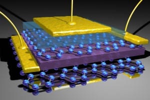
The device consists of two layers of graphene separated by an insulating layer of boron nitride just a few atomic layers thick. The electron clouds in each graphene layer can be tuned by applying a small voltage. This can induce the electrons into a state where they move spontaneously at high speed between the layers.
Because the insulating layer separating the two graphene sheets is ultra-thin, electrons are able to move through this barrier by ‘quantum tunnelling’. This process induces a rapid motion of electrical charge which can lead to the emission of high-frequency electromagnetic waves.
These new transistors exhibit the essential signature of a quantum seesaw, called negative differential conductance, whereby the same electrical current flows at two different applied voltages. The next step for researchers is to learn how to optimise the transistor as a detector and emitter.
One of the researchers, Professor Laurence Eaves, said: “In addition to its potential in medical imaging and security screening, the graphene devices could also be integrated on a chip with conventional, or other graphene-based, electronic components to provide new architectures and functionality.

“For more than 40 years, technology has led to ever-smaller transistors; a tour de force of engineering that has provided us with today’s state-of-the-art silicon chips which contain billions of transistors. Scientists are searching for an alternative to silicon-based technology, which is likely to hit the buffers in a few years’ time, and graphene may be an answer.”
The Latest Bing News on:
Revolutionary transistor technology
- CORRECTION: VueReal Unveils ColourFusion(TM) microDisplay: A Revolution in Augmented Reality (AR) Display Technologyon May 8, 2024 at 8:07 am
WATERLOO, ON / ACCESSWIRE / May 8, 2024 / VueReal, a pioneer in MicroSolid Printing™, today announced the launch of its revolutionary ColourFusion™ microDisplay, an innovative augmented reality (AR) ...
- Semiconductor-electronics industry prods Ched to improve IT courseson May 8, 2024 at 4:49 am
THE semiconductor and electronics industry is prodding the Commission on Higher Education (CHED) to improve courses that would help meet the industry’s needs as the country plays catch-up with the ...
- Robert Dennard, inventor of DRAM and pioneer of semiconductor scaling, dies at 91on May 7, 2024 at 10:48 am
Dennard's claims to fame are enormous. He's the mind behind dynamic random-access memory (DRAM), the ubiquitous memory that quite literally makes our computers and smartphones function.
- Development Bank Backs Kubos Semiconductor’s Plans for New Micro-LEDson May 7, 2024 at 7:54 am
Semiconductor manufacturer Kubos is set to bring its revolutionary new compound semiconductor material to South Wales, thanks to a £670,000 equity ...
- Ultra-Pure Silicon Chip Sparks a Quantum Computing Revolutionon May 7, 2024 at 2:00 am
Researchers at the Universities of Melbourne and Manchester have invented a breakthrough technique for manufacturing highly purified silicon that brings powerful quantum computers a big step closer. T ...
- The Revolutionary Journey of Transistors: From Inception to Global Dominationon May 3, 2024 at 6:46 am
The transistor, often hailed as one of the most significant inventions of the 20th century, began its journey in the patent files long before it materialized into a working device. Initially conceived ...
- TSMC debuts silicon technologies at its North America Technology Symposiumon May 1, 2024 at 5:00 pm
Leading semiconductor foundry TSMC has this week unveiled ... It also introduced its System-on-Wafer (TSMC-SoW) technology, an innovative solution to bring revolutionary performance to the wafer level ...
- Semicon ecosystem: A revolution in Indiaon April 30, 2024 at 7:26 pm
India's talent, resources and infrastructure position it to excel in the semiconductor sector and becoming a global leader As our lives become increasingly reliant on technology, semiconductors have ...
- Organic electrochemical transistors: Scientists solve chemical mystery at the interface of biology and technologyon April 30, 2024 at 11:22 am
Researchers who want to bridge the divide between biology and technology spend a lot of time thinking about translating between the two different "languages" of those realms.
- Semiconductor Technology: Driving the Digital Revolutionon April 30, 2024 at 7:26 am
Semiconductor technology is the foundation of modern electronics, enabling the development of devices such as transistors, integrated circuits, and microprocessors. It involves the use of ...
The Latest Google Headlines on:
Revolutionary transistor technology
[google_news title=”” keyword=”revolutionary transistor technology” num_posts=”10″ blurb_length=”0″ show_thumb=”left”]
The Latest Bing News on:
Graphene-based transistor
- Wonder Material 'More Remarkable' Than Graphene Has Medical Potentialon May 7, 2024 at 8:55 am
Borophene is already thinner and more conductive than graphene, and scientists have altered it to make it even more special.
- Finnlines Adopts Graphene-based Hard Foul Release Hull Coatingon May 7, 2024 at 8:30 am
Finnlines has turned to a innovative graphene-based hard foul release hull coating to reduce fuel consumption and emissions ...
- Graphene in Biomedicine: Opportunities and Challengeson May 5, 2024 at 5:00 pm
Graphene, whose discovery won the 2010 Nobel Prize in physics, has been a shining star in the material science in the past few years. Owing to its interesting electrical, optical, mechanical and ...
- Tracking the opioid epidemicon May 4, 2024 at 5:00 pm
The novel device is the first to use graphene-based field effect transistors to detect four different synthetic and natural opioids at once, while shielding them from wastewater’s harsh elements. When ...
- Graphene at 20: why the ‘wonder material’ is finally coming goodon April 30, 2024 at 6:31 am
Strong, light and with amazing electronic properties, graphene has always been touted as the “wonder material”. But two decades after it was first isolated, James McKenzie believes the graphene is ...
- Georgia Tech group create world’s first graphene-based semiconductoron April 26, 2024 at 10:13 am
A group of researchers at the Georgia Institute of Technology (Georgia Tech) have created the world’s first functional semiconductor made from graphene, a development that could lead to advanced ...
- Paragraf provides access to its graphene technology via new online storeon April 14, 2024 at 5:00 pm
has opened a new online store to enable global access to its Graphene-based Field Effect Transistor (GFET). GFETs have a wide range of uses in the development of industry, medical, and chemical test ...
- From strength to strengthon March 31, 2024 at 9:56 am
the first graphene-based SET, and the bipolar superconducting transistor are just a few of many highlights. Moreover, the development of graphene-based nanoelectronics looks possible, if difficult.
- The Future of Electronics is Here: How Georgia Tech’s Innovative Graphene Chip Technology Transforms the Fieldon March 7, 2024 at 1:58 am
This new semiconducting material, known as semiconducting epitaxial graphene (SEC ... speeds 10 times faster than those of the silicon-based transistors found in current chips.
- New transistors based on monolayer black phosphorus and germanium arsenideon January 6, 2024 at 5:32 am
Most proposed monolayer transistors based on 2D semiconductors were created using a few carefully selected materials known to have relatively stable lattice structures, such as graphene ...
The Latest Google Headlines on:
Graphene-based transistor
[google_news title=”” keyword=”graphene-based transistor” num_posts=”10″ blurb_length=”0″ show_thumb=”left”]

