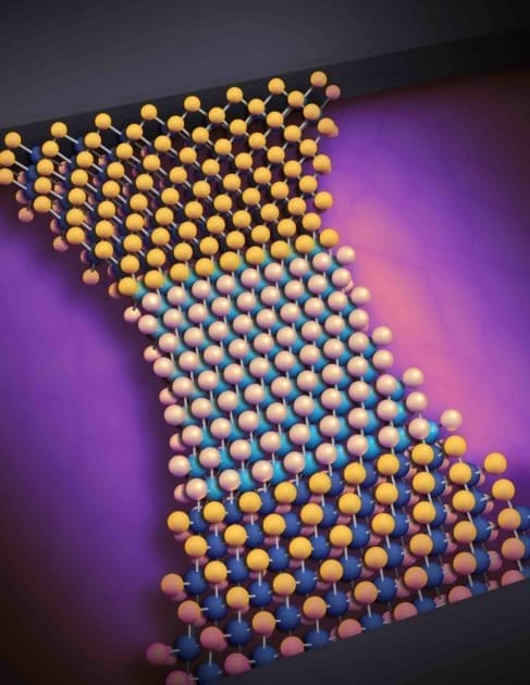
Two-dimensional (2D) materials—as thin as a single layer of atoms—have intrigued scientists with their flexibility, elasticity, and unique electronic properties since first being discovered in materials such as graphene in 2004. Some of these materials can be especially susceptible to changes in their material properties as they are stretched and pulled. Under applied strain, they have been predicted to undergo phase transitions as disparate as superconducting in one moment to nonconducting the next, or optically opaque in one moment to transparent in the next.
Now, University of Rochester researchers have combined 2D materials with oxide materials in a new way, using a transistor-scale device platform, to fully explore the capabilities of these changeable 2D materials to transform electronics, optics, computing, and a host of other technologies.
“We’re opening up a new direction of study,” says Stephen Wu, assistant professor of electrical and computer engineering and physics. “There’s a huge number of 2D materials with different properties—and if you stretch them, they will do all sorts of things.”
The platform developed in Wu’s lab, configured much like traditional transistors, allows a small flake of a 2D material to be deposited onto a ferroelectric material. Voltage applied to the ferroelectric—which acts like a transistor’s third terminal, or gate—strains the 2D material by the piezoelectric effect, causing it to stretch. That, in turn, triggers a phase change that can completely alter the way the material behaves. When the voltage is turned off, the material retains its phase until an opposite polarity voltage is applied, causing the material to revert to its original phase.
“The ultimate goal of two-dimensional straintronics is to take all of the things that you couldn’t control before, like the topological, superconducting, magnetic, and optical properties of these materials, and now be able to control them, just by stretching the material on a chip,” Wu says.
“If you do this with topological materials you could impact quantum computers, or if you do it with superconducting materials you can impact superconducting electronics.”
Maxing out Moore’s Law
In a paper in Nature Nanotechnology, Wu and his students describe using a thin film of two-dimensional molybdenum ditelluride (MoTe2) in the device platform. When stretched and unstretched, the MoTe2 changes from a low conductivity semiconductor material to a highly conductive semimetallic material and back again.
“It operates just like a field effect transistor. You just have to put a voltage on that third terminal, and the MoTe2 will stretch a little bit in one direction and become something that’s conducting. Then you stretch it back in another direction, and all of a sudden you have something that has low conductivity,” Wu says.
The process works at room temperature, he adds, and, remarkably, “requires only a small amount of strain—we’re stretching the MoTe2 by only 0.4 percent to see these changes.”
Moore’s Law famously predicts that the number of transistors in a dense, integrated circuit will double about every two years.
Yet technology is nearing the limits at which traditional transistors can be scaled down in size. So, as we reach the limits of Moore’s Law, the technology developed in Wu’s lab could have far-reaching implications in moving past these limitations in the quest for ever faster, more enhanced computing power.
Wu’s platform has the potential to perform the same functions as a transistor with far less power consumption since power is not needed to retain the conductivity state. Moreover, it minimizes the leakage of electrical current due to the steep slope at which the device changes conductivity with applied gate voltage. Both of these issues—high power consumption and leakage of electrical current—have constrained the performance of traditional transistors at the nanoscale.
“This is the first demonstration,” Wu adds. “Now it’s up to researchers to figure out how far it goes.”
No strain, no gain
One advantage of Wu’s platform is that it is configured much like a traditional transistor, making it easier to eventually adapt into current electronics. However, more work is needed before the platform reaches that stage. Currently, the device can operate only 70 to 100 times in the lab before device failure. While the endurance of other non-volatile memories, like flash, are much higher, they also operate much slower than the ultimate potential of the strain-based devices being developed in Wu’s lab.
“Do I think it’s a challenge that can be overcome? Absolutely,” says Wu, who will be working on the problem with Hesam Askari, an assistant professor of mechanical engineering at Rochester, also a coauthor on the paper. “It’s a materials engineering problem that we can solve as we move forward in our understanding how this concept works.”
They will also explore how much strain can be applied to various two-dimensional materials without causing them to break. Determining the ultimate limit of the concept will help guide researchers to other phase-change materials as the technology moves forward.
Learn more: Researchers ‘stretch’ the ability of 2D materials to change technology
The Latest on: Two-dimensional straintronics
[google_news title=”” keyword=”two-dimensional straintronics” num_posts=”10″ blurb_length=”0″ show_thumb=”left”]
via Google News
The Latest on: Two-dimensional straintronics
- The fusion of two sisters into a single woman suggests that human identity is not in our DNAon May 8, 2024 at 1:48 am
The biologist Alfonso Martínez Arias defends that genes do not define the uniqueness of a person, citing the example of Karen Keegan, who has two genomes ...
- The Best Two-Factor Authentication Appon April 27, 2024 at 9:47 am
Along with using a password manager, the most important thing you can do to secure your online accounts is to enable two-factor authentication (2FA) everywhere you can. After testing 10 2FA apps ...
- Two-dimensional materials articles from across Nature Portfolioon April 24, 2024 at 5:00 pm
Two-dimensional materials are substances with a thickness of a few nanometres or less. Electrons in these materials are free to move in the two-dimensional plane, but their restricted motion in ...
- Study shows ultra-thin two-dimensional materials can rotate the polarization of visible lighton April 22, 2024 at 8:52 am
It has been known for centuries that light exhibits wave-like behavior in certain situations. Some materials are able to rotate the polarization, i.e. the direction of oscillation, of the light wave ...
- Two-dimensional nanomaterial sets expansion recordon April 16, 2024 at 5:01 pm
"We were specifically looking to create a two-dimensional nanomaterial from tungsten semi-carbide," said Stocek. "In 2018, theorists predicted that it might exhibit this behavior to an excellent ...
- Two-Dimensional Random Walkon January 11, 2024 at 4:39 pm
Berestycki, Nathanaël Lis, Marcin and Qian, Wei 2023. Free boundary dimers: random walk representation and scaling limit. Probability Theory and Related Fields, Vol ...
- 2-dimensional shapes - AQAon July 25, 2020 at 9:11 pm
To calculate the perimeter, label and add up the length of each side. This shape is made from two rectangles. What is the perimeter of this shape? First, calculate the missing lengths \(x\) and \(y\).
- 2-dimensional shapes - Edexcelon July 25, 2020 at 9:11 pm
The perimeter is the total distance around the edge of a 2D shape. Examples of units of distance are millimetres (mm), centimetres (cm) and metres (m). The perimeter of any 2D shape can be found ...
- The Two-Dimensional Stepper Motoron May 9, 2019 at 4:39 am
The design of this stepper motor is simply two coils of wire, with the X axis of the grid placed on the top copper layer of the PCB and the Y axis on the bottom copper layer. There are four poles ...
- Sculpture-Dimensional Studieson January 11, 2019 at 7:58 am
The Sculpture/Dimensional Studies two-year program is highly competitive; five Sculpture/Dimensional Studies students are admitted annually; two of whom work in glass art. Each accepted MFA candidate ...
via Bing News


