


New manufacturing process will enable photonic communication in consumer devices
A new microchip technology capable of optically transferring data could solve a severe bottleneck in current devices by speeding data transfer and reducing energy consumption by orders of magnitude, according to an article published in the April 19, 2018 issue of Nature.
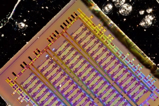
Researchers from Boston University, Massachusetts Institute of Technology, the University of California Berkeley and University of Colorado Boulder have developed a method to fabricate silicon chips that can communicate with light and are no more expensive than current chip technology.
The electrical signaling bottleneck between current microelectronic chips has left light communication as one of the only options left for further technological progress. The traditional method of data transfer–electrical wires–has a limit on how fast and how far it can transfer data. It also uses a lot of power and generates heat. With the relentless demand for higher performance and lower power in electronics, these limits have been reached. But with this new development, that bottleneck can be solved.
“Instead of a single wire carrying around 10 gigabits per second, you can have a single optical fiber carrying 10 to 20 terabits per second—so a thousand times more in the same footprint,” says Assistant Professor Milos Popovic (ECE), one of the principal investigators of the study, whose team was previously at University of Colorado Boulder where part of the work was done.
“If you replace a wire with an optical fiber, there are two ways you win,” he says. “First, with light, you can send data at much higher frequencies without significant loss of energy as there is with copper wiring. Second, with optics, you can use many different colors of light in one fiber and each one can carry a data channel. The fibers can also be packed more closely together than copper wires can without crosstalk.”
In the past, progress to integrate a photonic capability onto state-of-the-art chips that are used in computers and smartphones was hindered by a manufacturing roadblock. Modern processors are enabled by highly developed industrial semiconductor manufacturing processes capable of stamping out a billion transistors that work together on one chip. But these manufacturing processes are finely tuned and designing an approach to include optical devices on chips while keeping the current electrical capabilities intact proved difficult.
The first major success in overcoming this roadblock was in 2015 when the same group of researchers published another paper in Nature that solved this problem, but in a limited commercially relevant setting. The paper demonstrated the world’s first microprocessor with a photonic data transfer capability and the approach to manufacturing it without changing the industrial manufacturing process–a concept the researchers have termed a zero-change technology. Ayar Labs, Inc., a startup of which Popovic is a co-founder and technical advisor, has recently partnered with major semiconductor industry manufacturer GlobalFoundries to commercialize this technology.
Although this initial solution promises significant commercial impact, especially in the data communication sector, its ultimate applicability is limited because of the high cost of its starting material—silicon-on-insulator. To develop a solution for all silicon microelectronics, the researchers needed to focus their efforts on using the predominant, low-cost starting substrate—bulk silicon. Bulk silicon is used to make the majority of common microchips, and is what’s in laptops and smartphones. Silicon-on-insulator delivers a higher performance than bulk silicon, but at a significant cost premium and as such is primarily used in certain high-end microprocessors.
The difference between bulk silicon and silicon-on-insulator is that the latter has a layer of insulator, typically very pure glass, directly underneath a thin layer of silicon and the former doesn’t. The glass acts as a barrier for light particles to keep them confined in optical waveguides in the device. Without the glass barrier, the light signal would be lost.
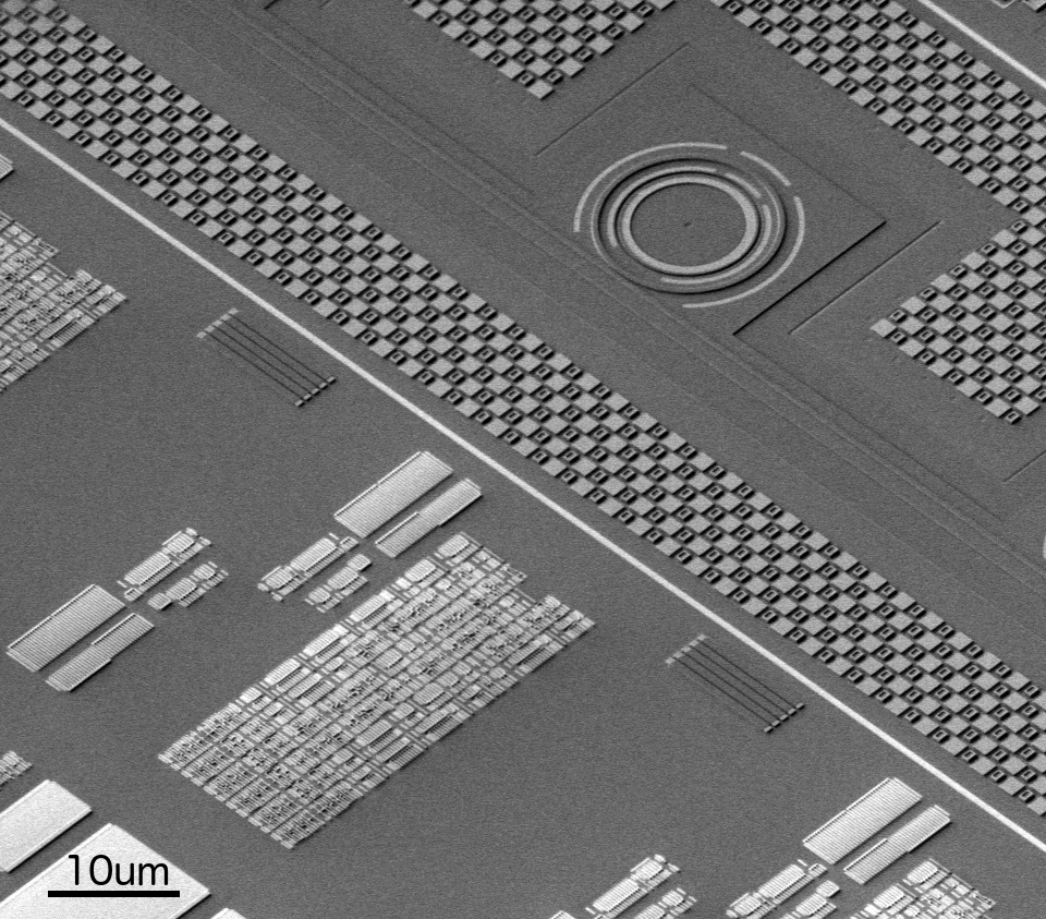
In the most recent paper, the researchers present a manufacturing solution by introducing a set of new material layers in the photonic processing portion of a bulk silicon chip. They demonstrate that this change allows optical communication with no impact on electronics. By working with industrial semiconductor manufacturing researchers at the Colleges of Nanoscale Science and Engineering of the State University of New York at Albany to develop this solution, the scientists ensured that any process that was developed could be seamlessly inserted into current industry-level manufacturing. The result crowns a several-year-long project funded by the Defense Advanced Research Project Agency and led initially by Associate Professor Vladimir Stojanovic of UC Berkeley and more recently by Professor Rajeev Ram of MIT, Popovic’s collaborators on the project.
“By carefully investigating and optimizing the properties of the additional material layers for photonic devices, we managed to demonstrate state-of-the-art system-level performance in terms of bandwidth density and energy consumption while starting from a much less expensive process compared to competing technologies,” says Fabio Pavanello, a former postdoctoral associate from Popovic’s research group who is a co-first author of the paper with both Amir Atabaki, a postdoctoral associate at MIT, and Sajjad Moazeni, a graduate student at UC Berkeley. Pavanello led the photonic transmitter device design and chip assembly in the project.

The new platform, which brings photonics to state-of-the-art bulk silicon microelectronic chips, promises faster and more energy efficient communication that could vastly improve computing and mobile devices. Applications beyond traditional data communication include accelerating the training of deep-learning artificial neural networks used in image and speech recognition tasks, and low-cost infrared LIDAR sensors for self-driving cars, smartphone face identification and augmented reality technology. In addition, optically enabled microchips could enable new types of data security and hardware authentication, more powerful chips for mobile devices operating on 5th generation (5G) wireless networks, and components for quantum information processing and computing.
The Latest on: Electronic photonic chip
[google_news title=”” keyword=”electronic photonic chip” num_posts=”10″ blurb_length=”0″ show_thumb=”left”]
via Google News
The Latest on: Electronic photonic chip
- 74th ECTC in Denver May 28-31on April 30, 2024 at 10:01 pm
IEEE Electronic Components and Technology Conference (ECTC) will take place May 28-31, 2024 at Denver’s Gaylord Rockies Resort & ...
- ECTC 2024 to highlight emerging technologies enabling heterogeneous integration and photonicson April 30, 2024 at 10:55 am
The IEEE Electronic Components and Technology Conference (ECTC) is the world’s leading forum for unveiling, discussing, and exhibiting the latest advancements in microelectronics packaging and ...
- TSMC details 12.8 Tbps on-package communication solution — an efficient silicon photonics interconnect for AIon April 30, 2024 at 10:44 am
TSMC goes optical with a 3D stacked silicon photonics interconnect called COUPE — Compact Universal Photonic Engine. It could deliver up to 12.8 Tbps of on-package connectivity for future chip designs ...
- POET Announces Additional Private Placement Financing for CAD$10 Millionon April 29, 2024 at 2:40 pm
NOT FOR DISTRIBUTION TO U.S. NEWS WIRE SERVICES OR FOR DISSEMINATION IN THE UNITED STATESTORONTO, April 29, 2024 (GLOBE NEWSWIRE) -- POET ...
- Photons Frozen in Time by Innovative Crystal Designson April 29, 2024 at 9:13 am
AMOLF researchers, in collaboration with Delft University of Technology, succeeded in bringing light waves to a halt by deforming the two-dimensional photonic crystal that contains them. The ...
- TSMC lays out roadmap for massive, kilowatt-class chip packages and terabit optical linkson April 29, 2024 at 6:09 am
Starting with the chip packaging tech, which TSMC has branded "CoWoS" (Chip-on-Wafer-on-Substrate), it's essentially an enhanced version of typical chiplet designs, where multiple smaller dies are ...
- POET Announces CAD$10 Million Non-brokered Financingon April 29, 2024 at 6:00 am
NOT FOR DISTRIBUTION TO U.S. NEWS WIRE SERVICES OR FOR DISSEMINATION IN THE UNITED STATESTORONTO, April 29, 2024 (GLOBE NEWSWIRE) -- POET ...
- This AI-focused chip is powered by lighton April 27, 2024 at 3:01 am
Called Taichi, this photonic AI chip is also particularly ... up to 1,000 times more energy efficient than a traditional electronic chip. The Taichi chip represents a major innovation in the ...
- Ansys (ANSS) Announces Strategic Collaboration With TSMCon April 25, 2024 at 6:21 am
Ansys (ANSS) joins forces with TSMC for the development of multiphysics software for TSMC's Compact Universal Photonic Engines - an advanced Silicon Photonics integration system.
via Bing News
